Supercharge Your Innovation With Domain-Expert AI Agents!

Image sensor and fabricating method thereof

An image sensor and photosensitive device technology, applied in the field of image sensors, can solve the problems of dark current, lack of photosensitivity, protection of heat-sensitive structures, etc.

Inactive Publication Date: 2010-03-10
SAMSUNG ELECTRONICS CO LTD
View PDF13 Cites 8 Cited by
  • Summary
  • Abstract
  • Description
  • Claims
  • Application Information

AI Technical Summary

Problems solved by technology

However, current backside image sensor designs and fabrication processes suffer from various drawbacks such as dark current, lack of photosensitivity (i.e., low quantum efficiency), and the need to protect heat-sensitive structures during fabrication.

Method used


Image

  • Image sensor and fabricating method thereof
  • Image sensor and fabricating method thereof
  • Image sensor and fabricating method thereof

Examples


Embodiment Construction

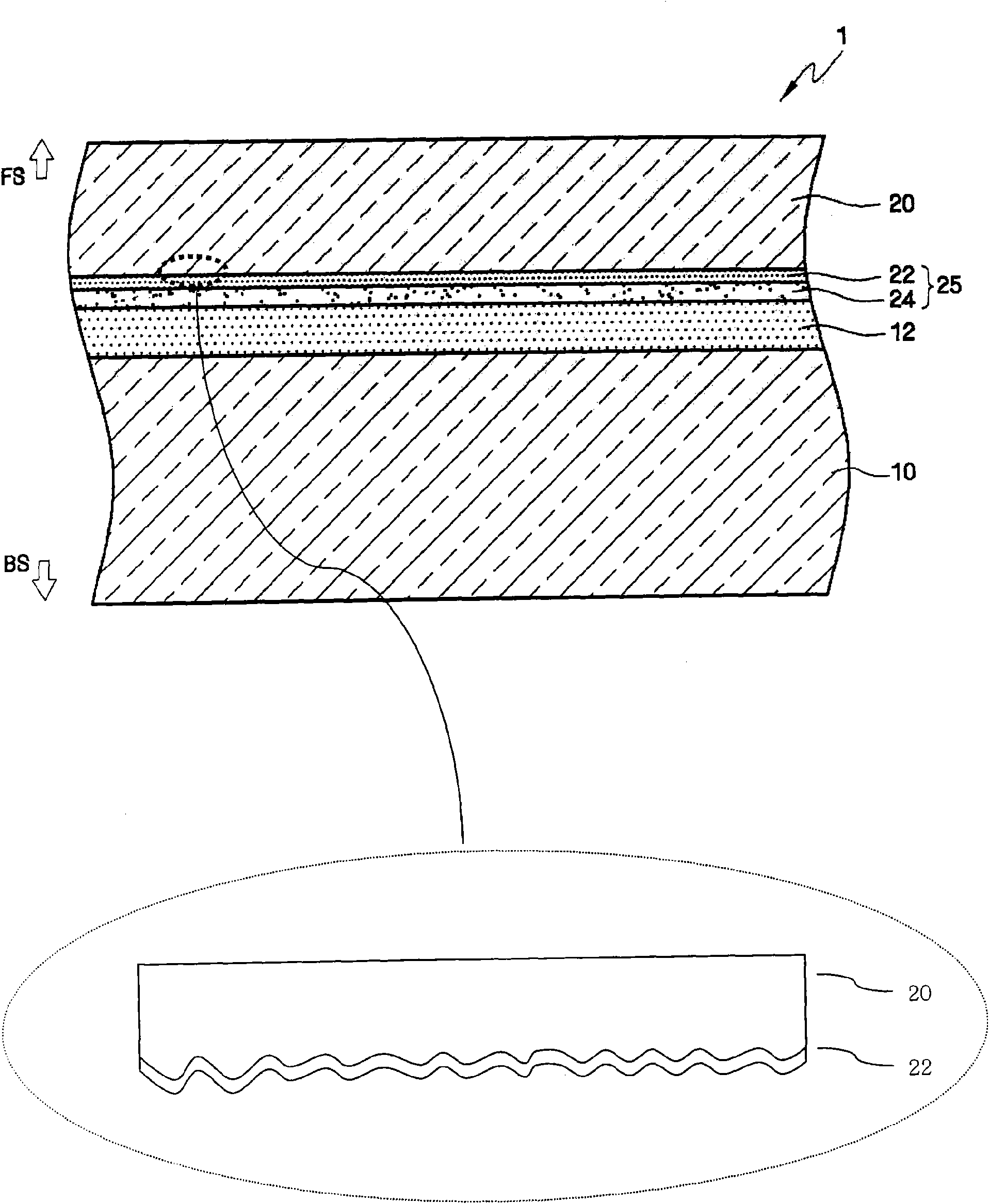
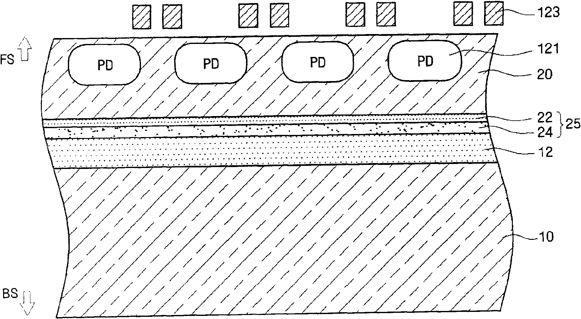
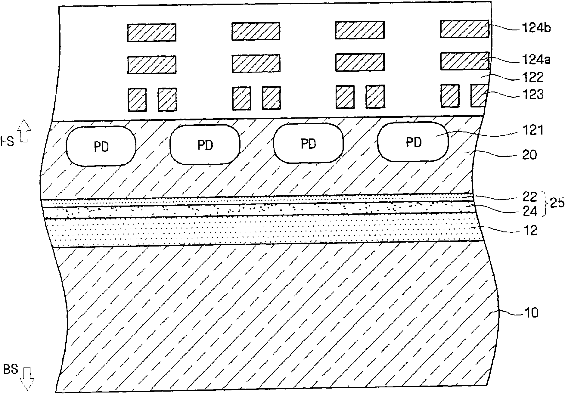
[0054] Example embodiments will be described more fully hereinafter with reference to the accompanying drawings; however, they may be embodied in different forms and should not be construed as limited to the embodiments set forth herein. Rather, these embodiments are provided so that this disclosure will be thorough and complete, and will fully convey the scope of the invention to those skilled in the art.

[0055] In the drawing figures, the dimensions of layers and regions may be exaggerated for clarity of illustration. It will also be understood that when a layer or element is referred to as being "on" another layer or substrate, it can be directly on the other layer or substrate, or intervening layers may also be present. Further, it will be understood that when a layer is referred to as being "under" another layer, it can be directly under, and one or more intervening layers may also be present. In addition, it will also be understood that when a layer is referred to as ...


PUM


Abstract

A method of fabricating a CMOS image sensor includes forming a substrate structure that includes a first substrate, a second substrate, and an index matching layer containing nitrogen and an oxide layer between the first and second substrates, and, forming at least one light-sensing device in the second substrate, and after forming the substrate structure, forming a metal interconnection structureon a first surface of the second substrate, the first surface facing away from the first substrate, such that the at least one light sensing device is between the metal interconnection structure andthe index matching layer and the oxide layer, the metal interconnection structure being electrically connected to the at least one light-sensing device.

Description

technical field [0001] Embodiments of the present invention relate to an image sensor, a substrate for the image sensor, an image sensing device including the image sensor, and related methods. Background technique [0002] The image sensor may be formed as a "front side" complementary metal oxide semiconductor (CMOS) image sensor that includes a plurality of photodiodes in a substrate. After forming the photodiodes, metal wiring patterns may be formed on the photodiodes. The metal wiring pattern may be formed to provide an opening for the photodiode to receive external light. However, light entering the opening at a certain angle is reflected by the metal wiring pattern. In addition, the interlayer dielectric layer surrounding the metal wiring pattern absorbs light incident thereon. Therefore, the amount of light passing through the opening to the photodiode may be reduced, resulting in poor device sensitivity. In addition, light reflected within the image sensor can af...

Claims


Application Information

Patent Timeline
IPC IPC(8): H01L21/50H01L21/82H01L27/146H01L23/12H04N5/335
CPCH01L2224/48227H01L27/1462H01L27/14685H01L27/1469
Inventor 朴炳俊金相熙
Owner SAMSUNG ELECTRONICS CO LTD
Features
  • R&D
  • Intellectual Property
  • Life Sciences
  • Materials
  • Tech Scout
  • Unparalleled Data Quality
  • Higher Quality Content
  • 60% Fewer Hallucinations
Learn More