

Method for making high alignment printed circuit board
A technology for printed circuit boards and manufacturing methods, which is applied to printed circuits, printed circuit manufacturing, and removal of conductive materials by chemical/electrolytic methods. problems, to achieve the effect of guaranteed quality, improved drilling accuracy, and smooth production
- Summary
- Abstract
- Description
- Claims
- Application Information
AI Technical Summary
Problems solved by technology
Method used
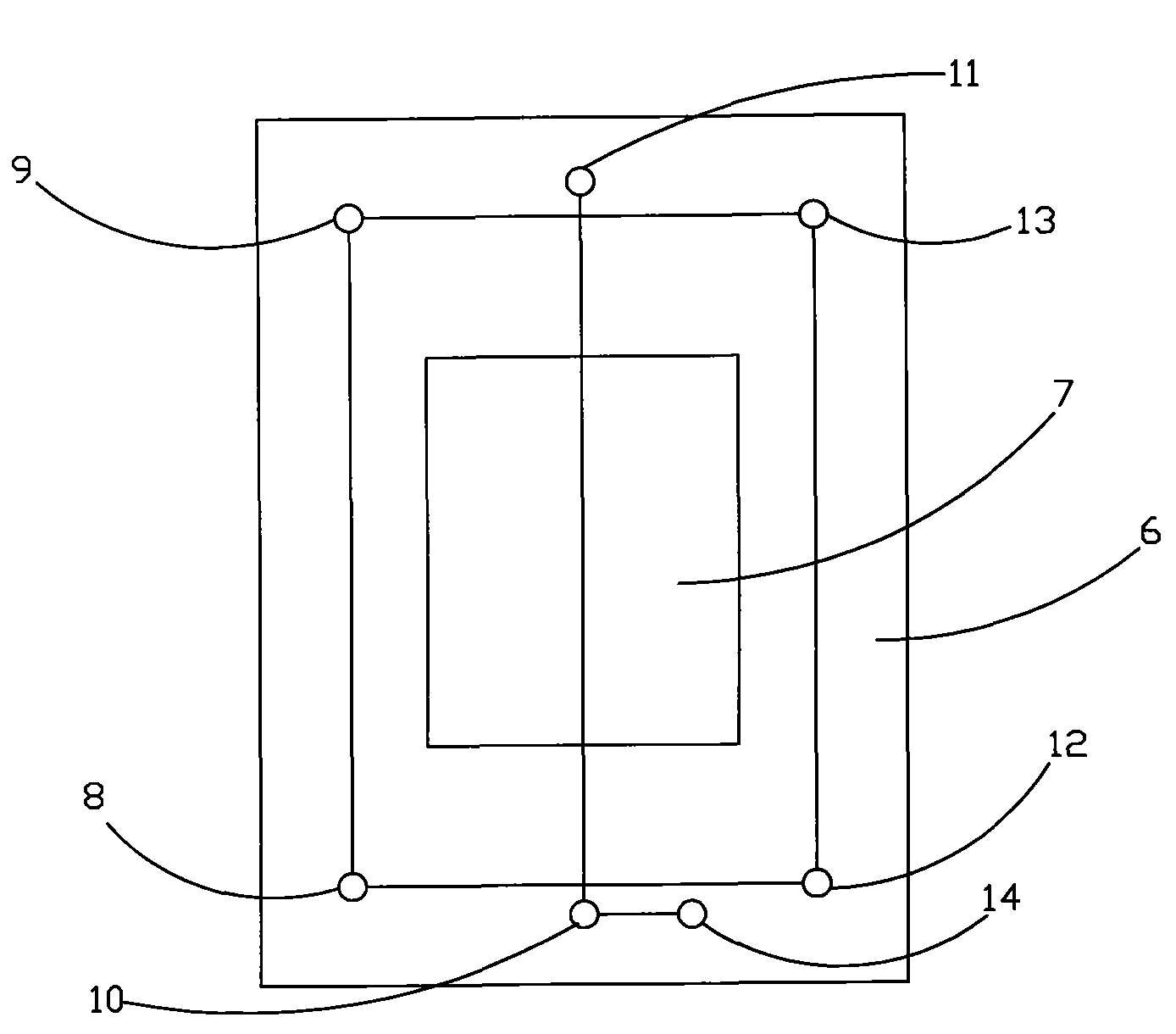
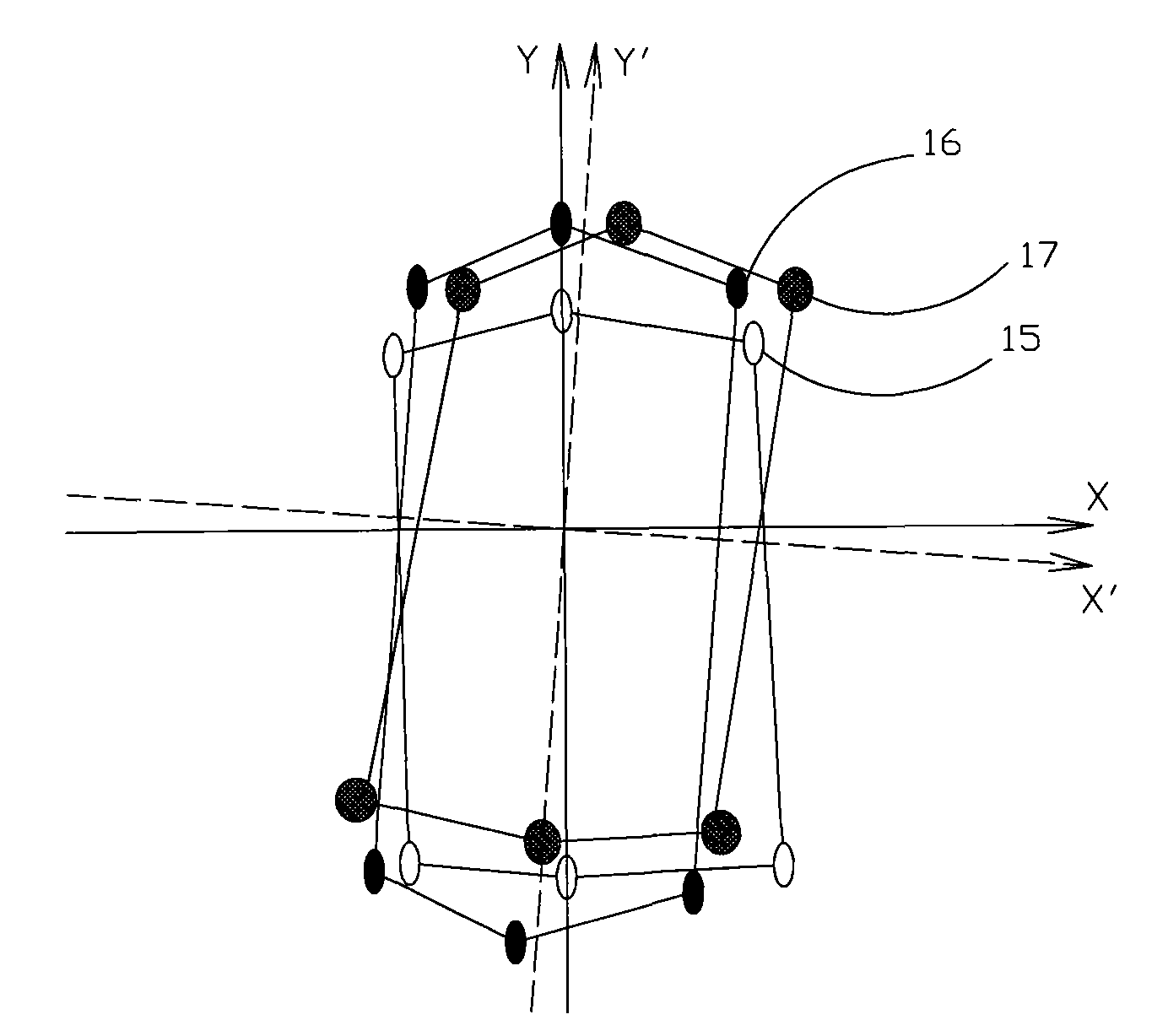
Image

Examples
Embodiment Construction
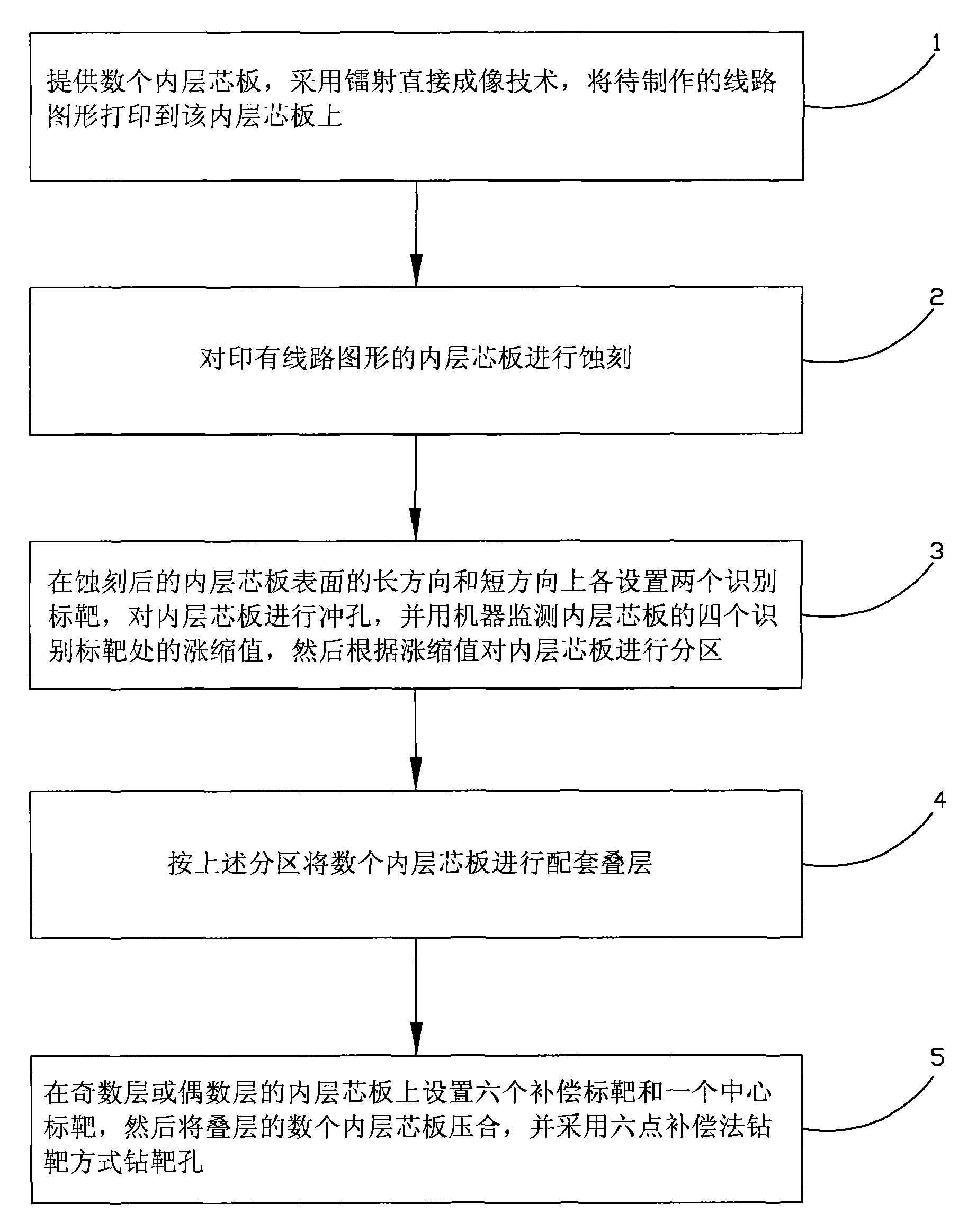
[0029] In order to further illustrate the technical means adopted by the present invention and its effects, the following describes in detail in conjunction with preferred embodiments of the present invention and accompanying drawings.
[0030] Such as figure 1 As shown, it is a flow chart of the manufacturing method of the high-alignment printed wiring board of the present invention, which includes the following steps:
[0031] Step 1: Provide several inner core boards, and use laser direct imaging technology to print the circuit pattern to be produced on the inner core boards. This step has changed the traditional way of using astigmatism or parallel light exposure machine for graphic transfer, using film for graphic exposure, using laser direct imaging technology, and calling the preset exposure graphic program, which can completely eliminate film shrinkage and other aspects The impact of the coincidence degree control accuracy is increased from the original ±50um to ±12....
PUM
 Abstract
Description
Claims
Application Information