Plasma enhanced chemical vapor deposition treatment method

A technology of chemical vapor deposition and plasma, which is applied in the direction of gaseous chemical plating, metal material coating process, coating, etc., can solve the problems of insufficient film tensile stress on the wafer substrate and the reduction of Mobility characteristics, so as to improve Mobility Properties, effect of increased tensile stress

Inactive Publication Date: 2010-03-17
SEMICONDUCTOR MANUFACTURING INTERNATIONAL (BEIJING) CORP
View PDF0 Cites 3 Cited by
  • Summary
  • Abstract
  • Description
  • Claims
  • Application Information

AI Technical Summary

Problems solved by technology

However, this method cannot remove the hydrogen in the free state on the surface of the film on the wafer substrate, that is, the hydrogen in the reaction furnace 100 every time the film on the wafer substrate is deposited, that is, steps 202 to 204, thereby affecting The tensile stress of the thin film on the final wafer substrate is not enough, resulting in a decrease in the Mobility characteristics of the final IC manufactured on the wafer

Method used


Image

  • Plasma enhanced chemical vapor deposition treatment method
  • Plasma enhanced chemical vapor deposition treatment method
  • Plasma enhanced chemical vapor deposition treatment method

Examples


Embodiment Construction

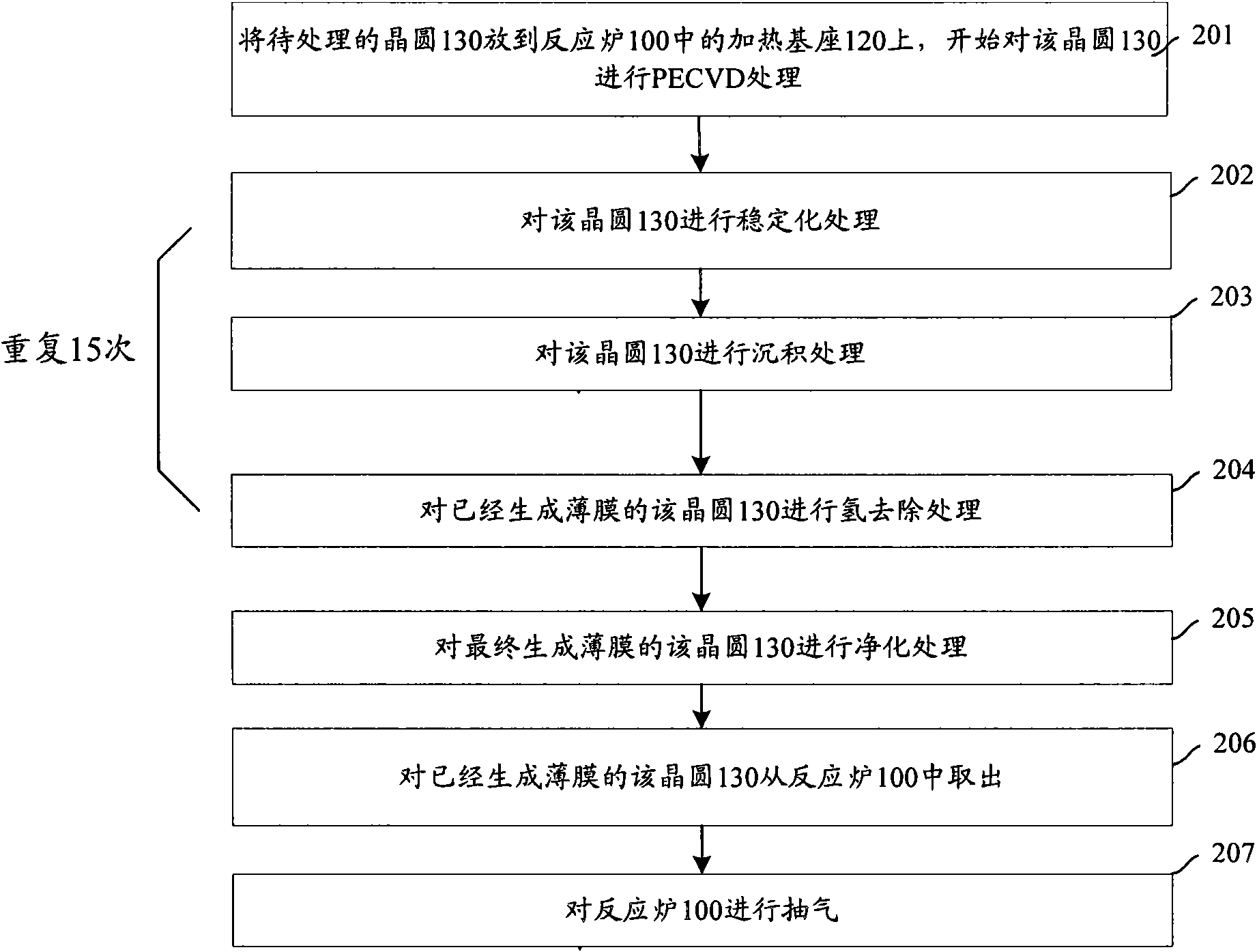
[0037] In order to make the object, technical solution and advantages of the present invention more clear, the present invention will be further described in detail by giving specific embodiments and referring to the accompanying drawings.

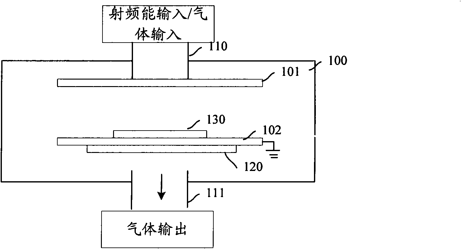
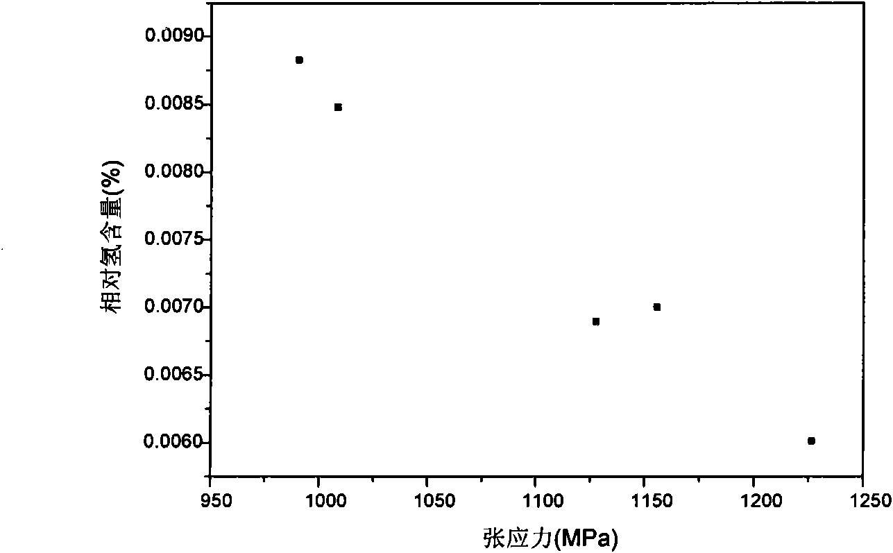
[0038] Such as image 3 as shown, image 3 It is a schematic diagram of the relationship between the hydrogen content in the reaction furnace 100 and the tensile stress of the film on the wafer substrate, wherein the abscissa is the tensile stress value of the film on the wafer substrate (in MPa), and the ordinate is the corresponding The relative hydrogen content in the reaction furnace 100 (unit is %), this is a relative value, not very accurate. From image 3 It can be seen from the figure that, for a thin film on a wafer substrate with the same thickness, the less hydrogen content in the reaction furnace 100 during the thin film deposition process, the greater the tensile stress of the thin film on the wafer substrate. Therefore, wh...


PUM

PropertyMeasurementUnit
thicknessaaaaaaaaaa
thicknessaaaaaaaaaa

Abstract

The invention discloses a plasma enhanced chemical vapor deposition treatment method which comprises the following steps: sequentially carrying out stabilizing treatment, depositing treatment, hydrogen removing treatment, purifying treatment and flaking treatment on a wafer substrate, and obtaining a thin film on the wafer substrate. The method also comprises the step of carrying out purifying treatment between the depositing treatment and the hydrogen removing treatment. When the method is used for depositing the thin film on the wafer substrate every time, the hydrogen content of the surfaceof the thin film is removed, thus the tension stress of the finally obtained thin film on the wafer substrate is increased.

Description

technical field [0001] The invention relates to the field of semiconductor manufacturing, in particular to a plasma-enhanced chemical vapor deposition treatment method. Background technique [0002] In the semiconductor manufacturing process, in order to arrange discrete devices and integrated circuits, different kinds of thin films need to be deposited on the substrate of the wafer. In the method of depositing thin films, plasma enhanced chemical vapor deposition (PECVD, Plasma Enhanced Chemical Vapor Deposition) is a commonly used method, which utilizes energy-enhanced chemical vapor deposition (CVD, Chemical Vapor Deposition) reaction to obtain crystal Films on round substrates. [0003] figure 1 A schematic diagram of an existing device for the PEVCD method is shown, and the device is a PECVD reactor 100 . The PECVD reaction furnace 100 is made of conical glass or aluminum, and the upper and lower ends are sealed with aluminum plates. There are two upper and lower pa...

Claims


Application Information

Patent Timeline
Patent Type & Authority Applications(China)
IPC IPC(8): C23C16/513
Inventor 徐强蔡明
Owner SEMICONDUCTOR MANUFACTURING INTERNATIONAL (BEIJING) CORP
Why Eureka
Try Eureka