Method of fabricating strained-silicon transistors

a technology of strained silicon and transistors, applied in the direction of semiconductor devices, electrical equipment, basic electric elements, etc., can solve the problems of difficult optimization of nmos and pmos transistors separately, the lithographic technology's limit of miniaturization, and the above technique still suffers, so as to increase the stress and move of electrons, the effect of rapid thermal annealing process

Active Publication Date: 2007-05-17
UNITED MICROELECTRONICS CORP
View PDF17 Cites 19 Cited by
  • Summary
  • Abstract
  • Description
  • Claims
  • Application Information

AI Technical Summary

Benefits of technology

[0011] It is therefore an objective of the present invention to provide a method of fabricating strained-silicon transistors for improving the conventional problem of being unable to effectively increase the electron mobility of NMOS transistors.
[0013] According to another aspect of the present invention, a method of fabricating strained-silicon transistors comprises: providing a semiconductor substrate, in which the semiconductor substrate comprises a gate, at least a spacer, and a source / drain region; removing the spacer and forming a high tensile stress film over the surface of the gate and the source / drain region; and performing a rapid thermal annealing process to simultaneously activate the dopants within the source / drain region and expand the lattice arrangement of the semiconductor substrate beneath the gate.
[0014] By utilizing the gate and spacer as a mask to implant the source / drain region, removing the spacer surrounding the gate, depositing a high tensile stress film over the surface of the gate and the source / drain region, and performing a rapid thermal annealing process, the present invention is able to increase the stress and movement of electrons of the strained-silicon transistor by expanding the lattice arrangement of the channel region within the semiconductor substrate.

Problems solved by technology

However, it has been recently pointed out that the miniaturization attained by a lithographic technology has reached its limit.
However, the above technique still suffers the following disadvantages.
First, the silicon germanium is deposited across the substrate, making it harder to optimize NMOS and PMOS transistors separately.
Second, the silicon germanium layer has poor thermal conductivity.
Moreover, despite the fact that the SiGe deposited into the predetermined source / drain region via a selective epitaxial growth (SEG) will increase the electron hole mobility of strained-silicon PMOS transistors, the process however will simultaneously decrease the electron mobility of NMOS transistors and influence the overall effectiveness of the transistor.

Method used


Image

  • Method of fabricating strained-silicon transistors
  • Method of fabricating strained-silicon transistors
  • Method of fabricating strained-silicon transistors

Examples


Embodiment Construction

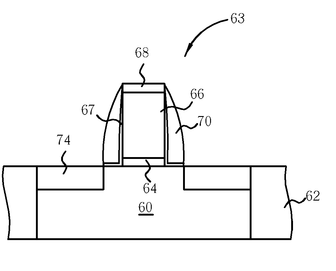
[0019] Please refer to FIG. 4 through FIG. 6. FIG. 4 through FIG. 6 are perspective diagrams showing the means of fabricating a strained-silicon PMOS transistor according to the present invention. As shown in FIG. 4, a semiconductor substrate 60, such as a silicon wafer or a silicon-on-insulator (SOI) substrate, is provided and a gate structure 63 is formed on the semiconductor substrate 60, in which the gate structure 63 includes a gate dielectric 64, a gate 66 disposed on the gate dielectric 64, a cap layer 68 formed on the gate 66, an oxide liner 67 disposed around the gate 66, and a spacer 70 formed on the oxide liner 67. Preferably, the gate dielectric 64 is composed of silicon dioxide via oxidation or deposition processes, the gate 66 is composed of doped polysilicon, and the cap layer 68 is composed of silicon nitride for protecting the gate 66 or polycide. Additionally, a shallow trench isolation (STI) 62 is formed around the active area of the gate structure 63 within the s...


PUM

PropertyMeasurementUnit
temperatureaaaaaaaaaa

Abstract

A method of fabricating strained-silicon transistors includes providing a semiconductor substrate, in which the semiconductor substrate includes a gate, at least a spacer, and a source / drain region; performing a first rapid thermal annealing (RTA) process; removing the spacer and forming a high tensile stress film over the surface of the gate and the source / drain region; and performing a second rapid thermal annealing process.

Description

BACKGROUND OF THE INVENTION [0001] 1. Field of the Invention [0002] The present invention relates to a method of fabricating semiconductor devices, and more particularly, to a method of fabricating strained-silicon transistors. [0003] 2. Description of the Prior Art [0004] The performance of MOS transistors has increased year after year with the diminution of critical dimensions and the advance of large-scale integrated circuits (LSI). However, it has been recently pointed out that the miniaturization attained by a lithographic technology has reached its limit. Therefore, how to improve the carrier mobility so as to increase the speed performance of MOS transistors has become a major topic for study in the semiconductor field. For the known arts, attempts have been made to use a strained silicon layer, which has been grown epitaxially on a silicon substrate with a silicon germanium (SiGe) layer disposed therebetween. In this type of MOS transistor, a biaxial tensile strain occurs in...

Claims


Application Information

Patent Timeline
Patent Type & Authority Applications(United States)
IPC IPC(8): H01L21/8234H01L21/425H01L21/336
CPCH01L29/6653H01L29/7843Y10S438/938
Inventor HUANG, CHENG-TUNGLIANG, CHIA-WENCHENG, TZYY-MINGSHEN, TZER-MINSHENG, YI-CHUNG
Owner UNITED MICROELECTRONICS CORP
Why Eureka
Try Eureka