Shift cache circuit

A shift register and circuit technology, applied in static memory, digital memory information, instruments, etc., can solve problems such as critical voltage drift, peak voltage Vrc1 increase, and reduced reliability and service life of the shift register circuit 100

A shift register and circuit technology, applied in static memory, digital memory information, instruments, etc., can solve problems such as critical voltage drift, peak voltage Vrc1 increase, and reduced reliability and service life of the shift register circuit 100

CN101673582AActive Publication Date: 2010-03-17AU OPTRONICS CORP

Image

  • Shift cache circuit
  • Shift cache circuit
  • Shift cache circuit

Examples


Embodiment Construction

[0039] In the following, according to the shift register circuit of the present invention, specific embodiments will be described in detail with the accompanying drawings, but the provided embodiments are not intended to limit the scope of the present invention.

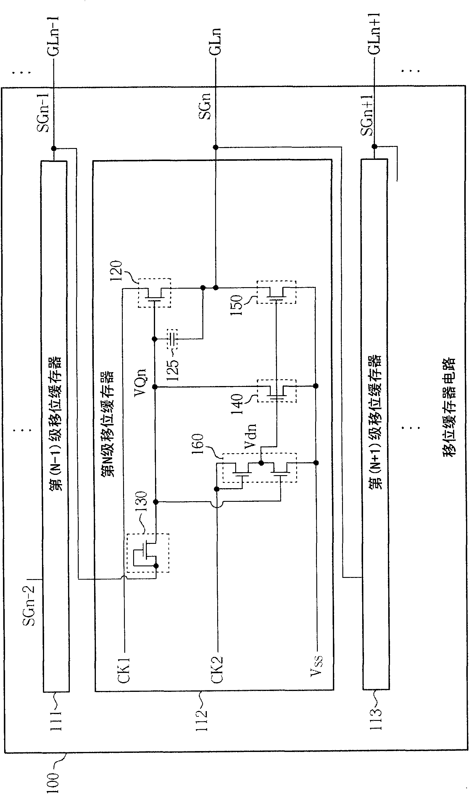
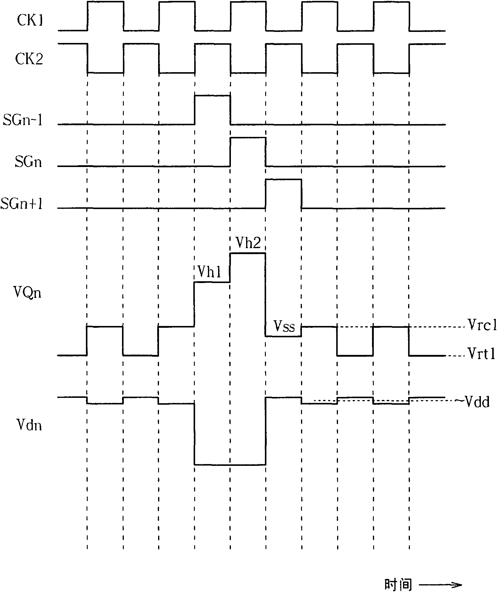
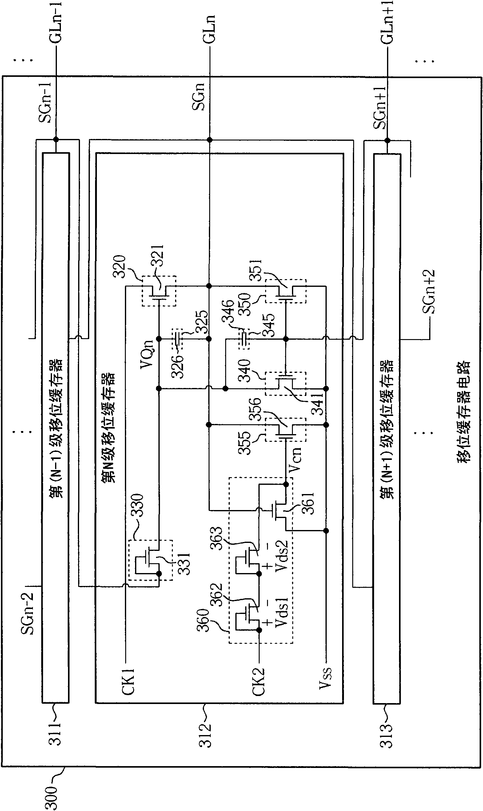
[0040] image 3It is a schematic diagram of the shift register circuit according to the first embodiment of the present invention. Such as image 3 As shown, the shift register circuit 300 includes a multi-stage shift register. For the convenience of illustration, the shift register circuit 300 only shows the (N-1)th stage shift register 311 and the Nth stage shift register 312. And the (N+1)th stage shift register 313, wherein only the N stage shift register 312 shows the internal functional unit structure, and the other stage shift registers are similar to the N stage shift register 312, so there is no Let me repeat. In the operation of the shift register circuit 300, the (N-1)th stage shift register 311 is used...


PUM


Abstract

The invention discloses a shift cache circuit. The shift cache circuit comprises a plurality of shift cache layer for providing a plurality of grid signals to a plurality of grid lines. Each layer of shift cache comprises a pull-up unit, an input unit for receiving an input signal, an energy storage unit for providing a drive control voltage according to the input signal, a discharge unit, a coupling unit and a pull-down unit. The pull-up unit pulls up a first grid signal according to the drive control voltage; the discharge unit is used for executing discharge action so as to pull down the drive control voltage; the coupling unit is used for coupling the energy storage unit with a post-layer shift cache so as to cause a second grid signal generated by the post-layer shift cache to drop with pull-down drive control voltage; and the pull-down unit pulls down the first grid signal according to the second grid signal.

Description

technical field [0001] The invention relates to a shift register circuit, in particular to a shift register circuit capable of reducing leakage current and voltage stress. Background technique [0002] A liquid crystal display (Liquid Crystal Display; LCD) is a flat panel display widely used at present, which has the advantages of light and thin appearance, power saving and no radiation. The working principle of the liquid crystal display device is to change the arrangement state of the liquid crystal molecules in the liquid crystal layer by changing the voltage difference between the two ends of the liquid crystal layer, so as to change the light transmittance of the liquid crystal layer, and cooperate with the light source provided by the backlight module to display images. Generally speaking, a liquid crystal display device includes a plurality of pixel units, a shift register circuit and a source driver. The source driver is used to provide multiple data signals to mult...

Claims


Application Information

Patent Timeline
17 Mar 2010
Publication
CN101673582A
IPC
G11C19/28; G11C27/04; G09G3/36
Inventors
刘晋炜; 吴威宪