Laser repair device and a laser repair method

A technology of laser repair and laser beam, which is applied in the field of defect repair, and can solve problems such as complex repair and pixel destruction

Inactive Publication Date: 2010-03-17
OLYMPUS CORP
View PDF2 Cites 24 Cited by
  • Summary
  • Abstract
  • Description
  • Claims
  • Application Information

AI Technical Summary

Problems solved by technology

Also, since the transparent electrode is transparent, the laser beam for repairing passes through the transparent electrode, and as a result, the laser beam reaches the metal wiring and the TFT, possibly causing the pixel to be destroyed.
Therefore, the restoration after forming the final layer requires technology to prevent pixel damage, and restoration is complicated

Method used


Image

  • Laser repair device and a laser repair method
  • Laser repair device and a laser repair method
  • Laser repair device and a laser repair method

Examples


Embodiment Construction

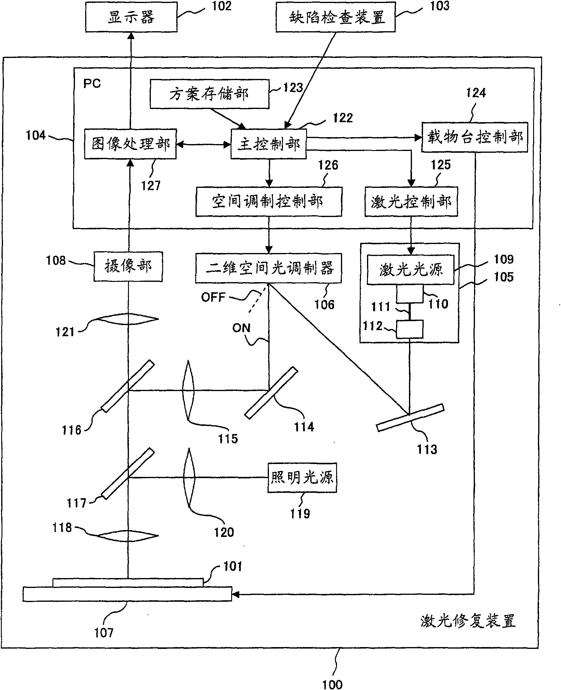
[0037] Hereinafter, embodiments of the present invention will be specifically described with reference to the drawings.

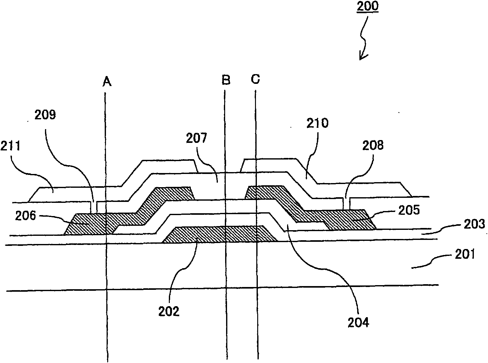
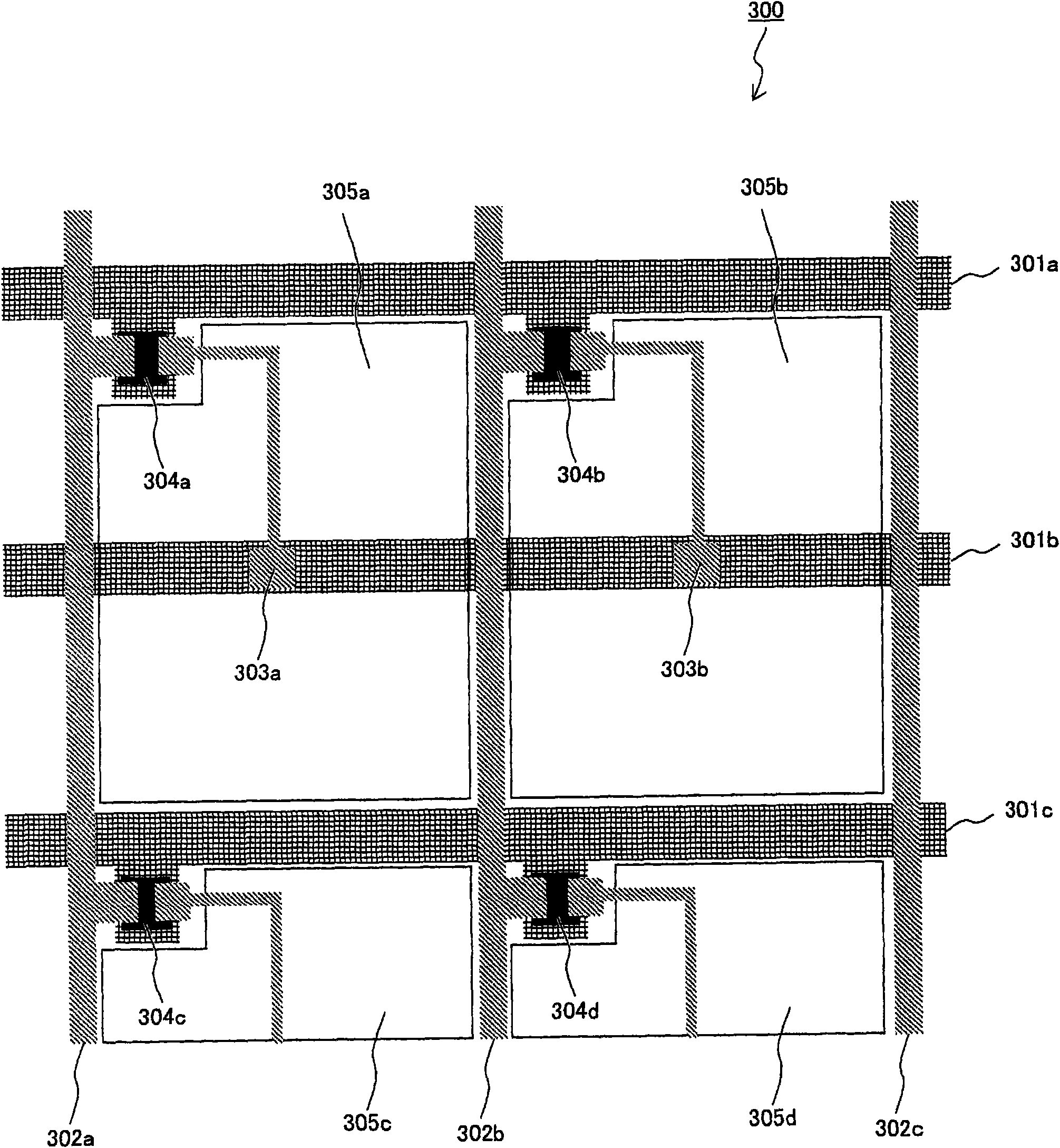
[0038] In addition, in the following embodiment, the term "glass substrate" and "FPD substrate" are differentiated and demonstrated as defined above. That is, a "glass substrate" is a base on which no substance is laminated, and an "FPD substrate" is a product in which various substances are laminated on a glass substrate. Simply referring to "substrate" refers to the glass substrate compared with the FPD substrate as a "product".

[0039] In addition, the "FPD substrate" as a "product" may be a semi-finished product in the middle of each manufacturing process of manufacturing a gate bus layer, an insulating film layer, an amorphous silicon layer, a source / drain bus layer, an insulating film layer, and a transparent electrode layer. , may also be a finished product after the manufacturing of each layer is formed. The object of laser repair in the followin...


PUM


Abstract

The invention discloses a laser repair device and a laser repair method, which can extremely precisely control irradiation of the laser beam and repair defect more appropriately. In the invention, a scheme storage part (123) stores irradiation condition image, and the irradiation condition image makes irradiation condition corresponding to a overlapping substance corresponds to each of a pluralityof overlapping areas on surface of a glass cardinal plate; a image processing part (127) that recognizes defect scope on surface of a FPD cardinal plate (101) manufactured through overlapping varioussubstance on the glass cardinal plate, and divides the defect scope as irradiation area according to irradiation condition image and which overlapping area is coincided; a master control part (122) that assigns more than one space modulation mode to a two dimensional space light modulator (106) by a laser control part (125) and a space modulation and control part (126) in series, so as to irradiate laser beam to the irradiation area according to irradiation condition of the irradiation area corresponding to overlapped area.

Description

technical field [0001] The present invention relates to a technique for repairing a defect by irradiating a laser beam to a defect on the surface of a product manufactured by laminating one or more substances for forming a circuit on the surface of a substrate. Background technique [0002] In the manufacturing process of FPD (Flat Panel Display: Flat Panel Display), for example, patterning is repeatedly performed using a photolithography process using a plurality of photomasks, and electrode patterns are formed on a glass substrate using etching technology and / or sputtering technology And / or TFT (Thin Film Transistor: Thin Film Transistor). In particular, TFT substrates for liquid crystal displays (LCD: Liquid Crystal Display) are used to form gate bus line layers, insulating film layers, amorphous silicon layers, and source-drain bus line layers. , 4 to 5 masks of the insulating film layer and the transparent electrode layer to manufacture the TFT substrate. In addition ...

Claims


Application Information

Patent Timeline
Patent Type & Authority Applications(China)
IPC IPC(8): H01L21/00H01L21/321B23K26/06G02B26/08B23K26/00B23K26/03B23K26/352G02F1/13
CPCG02F1/1303G02F1/1309
Inventor 赤羽隆之
Owner OLYMPUS CORP
Why Eureka
Try Eureka