


Quick Research
Generate reliable direction feasibility study reports for your R&D in just a few steps.

Technical Q&A
Discover and master advanced knowledge NOW. Basics, ideas, possibilities, all at once.

Find Solutions
As an expert in R&D theories, this can generate solutions to your technical problems instantly.

Evaluate Feasibility
Analyze your overall solution with one click, know your potential R&D risks in advance.

Monitor Landscape
Get weekly tech updates, stay abreast of the latest tech innovations and key insights.
Semiconductor package and method for manufacturing the same
A technology for packaging components and manufacturing methods, applied in semiconductor/solid-state device manufacturing, semiconductor devices, semiconductor/solid-state device components, etc., capable of solving problems such as failure of semiconductor package components 40, peeling of optical filters 46, etc.
- Summary
- Abstract
- Description
- Claims
- Application Information
AI Technical Summary
Problems solved by technology
Method used
Image

Examples
no. 1 Embodiment approach
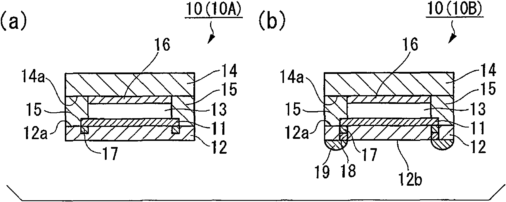
[0036] figure 1 It is a cross-sectional view showing the first embodiment of the semiconductor package of the present invention.
[0037] In the semiconductor package 10A, the semiconductor device 11 is arranged on one surface 12 a of the semiconductor substrate 12. On this semiconductor substrate 12, a cover substrate 14 is arranged to face each other with a gap 13 therebetween. In addition, the spacer 15 is protrudingly provided on the surface 14 a facing the semiconductor substrate 12 to bond the semiconductor substrate 12 and the cover substrate 14. In addition, the optical filter 16 is arranged on one surface 14 a of the cover substrate 14 so as to overlap with the semiconductor device 11 and not overlap with the spacer 15.
[0038] As for the semiconductor device 11, image sensors such as CCD and CMOS are ideal. In addition, MEMS (Micro Electro Mechanical System) devices and the like can also be used. Examples thereof include micro relays, micro switches, pressure sensors,...
no. 2 Embodiment approach
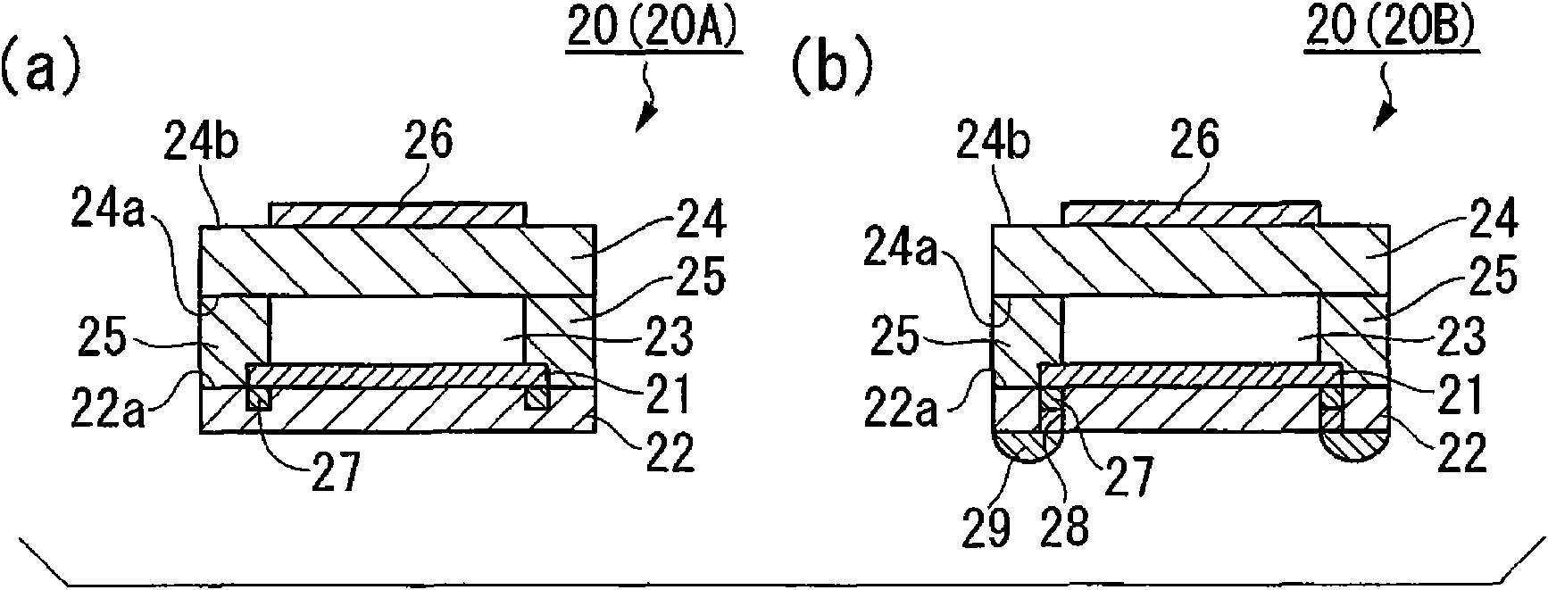
[0051] Such as image 3 As shown, in the present invention, the filter 26 may be arranged on the other surface 24b side of the cover substrate 24. In this case, the filter 26 may be directly arranged on the other surface 24b of the cover substrate 24, or the filter 26 may be provided via a layer arranged on the other surface 24b of the cover substrate 24. In addition, since the position where the filter 26 is arranged does not overlap with the cutting part, it will not be affected by debris during cutting. In addition, since it is not in contact with the spacer 25, peeling of the filter 26 due to the expansion and contraction stress of the spacer 25 that has occurred in the past can be avoided. Since the filter 26 is provided on the outer periphery of the semiconductor package 20, it can block unwanted light incident on the semiconductor device 21 before being incident on the semiconductor package 20.
no. 3 Embodiment approach
[0053] Such as Figure 5 As shown, in the present invention, the filter 36 may be arranged on both sides of one surface 34a and the other surface 34b of the cover substrate. That is, the semiconductor substrate 32, the first filter 36a, the cover substrate 34, and the second filter 36b are arranged to overlap in this order. Regarding the arrangement of the first filter 36a and the second filter 36b, it may be directly arranged on the cover substrate 34, or may be arranged indirectly via a layer arranged on the cover substrate 34. In any case, as in the above two embodiments, since the first filter 36a and the second filter 36b are arranged at a position that does not overlap the spacer 35, it is possible to prevent breakage due to cutting. Filter peeling caused by debris. Also, since the spacer 35 is not directly adhered to the two filters 36a and 36b as in the above-mentioned embodiment, it is also possible to prevent the filters 36 from peeling due to the expansion and contr...
PUM
 Abstract
Description
Claims
Application Information
 - R&D Engineer
- R&D Manager
- IP Professional
- Industry Leading Data Capabilities
- Powerful AI technology
- Patent DNA Extraction
Browse by: Latest US Patents, China's latest patents, Technical Efficacy Thesaurus, Application Domain, Technology Topic, Popular Technical Reports.
© 2024 PatSnap. All rights reserved.Legal|Privacy policy|Modern Slavery Act Transparency Statement|Sitemap|About US| Contact US: help@patsnap.com