Antistatic tool
An anti-static, appliance technology, applied in the direction of static electricity, applications, circuits, etc., can solve problems such as the inability to fully solve the compression marks, and achieve reliable anti-static properties, good adhesion, and prevent explosions.
- Summary
- Abstract
- Description
- Claims
- Application Information
AI Technical Summary
Problems solved by technology
Method used
Image
Examples
Embodiment 1
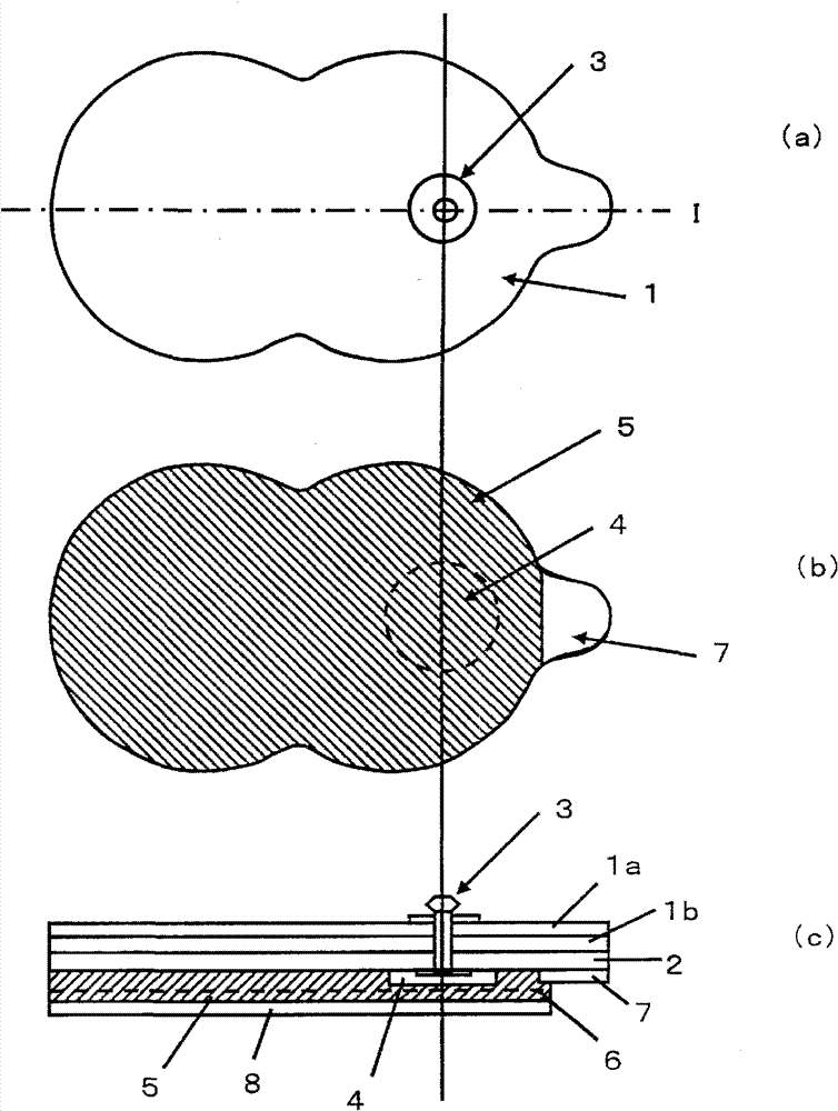
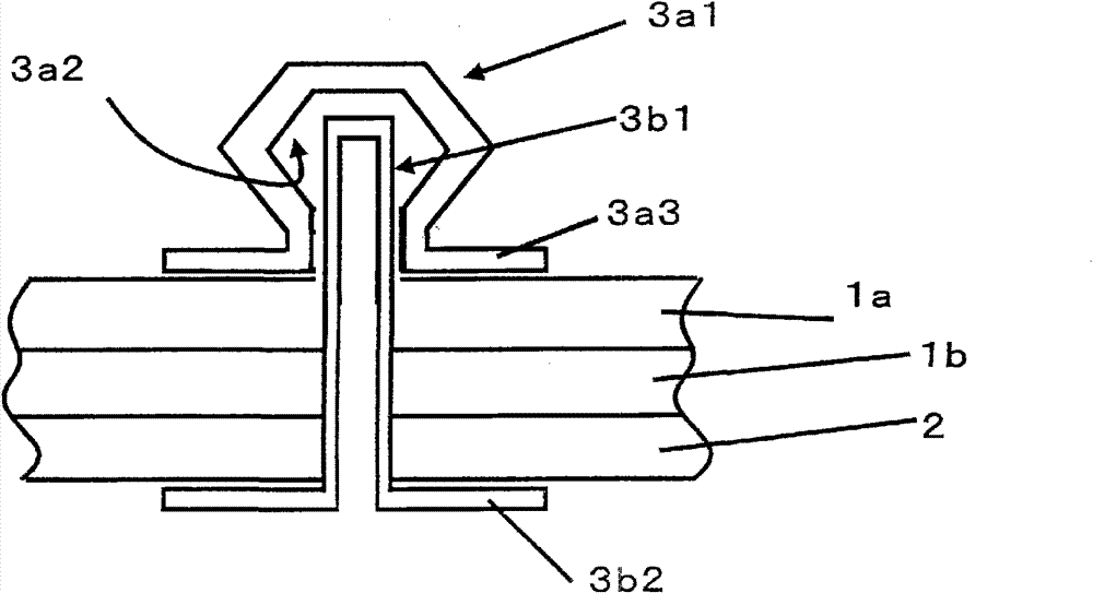
[0105] figure 1 (a)~(c) and figure 2 A schematic diagram of the antistatic appliance of Example 1 is shown in . figure 1 (a) is the top view schematic diagram of the antistatic appliance of embodiment 1, figure 1 (b) is the rear view schematic diagram of the antistatic appliance of embodiment 1, figure 1 (c) is the schematic sectional view of the I-I line of the antistatic appliance of embodiment 1, figure 2 yes figure 1 (c) An enlarged schematic view of the terminal portion. In addition, in figure 1 (a)~(c) and figure 2 Among them, reference numeral 1 is a supporting member, 1a is a soft polyethylene layer, 1b is a polyester film, 2 is a conductive layer, 3 is a terminal part, 3a is a conductive snap button, 3b is a conductive part, 4 is a cover layer, 5 is the conductive adhesive layer, 6 is the intermediate substrate, 7 is the non-adhesive layer, 8 is the protective film, 3a1 is the convex part of the conductive snap, 3a2 is the concave part of the conductive snap...
Embodiment 2
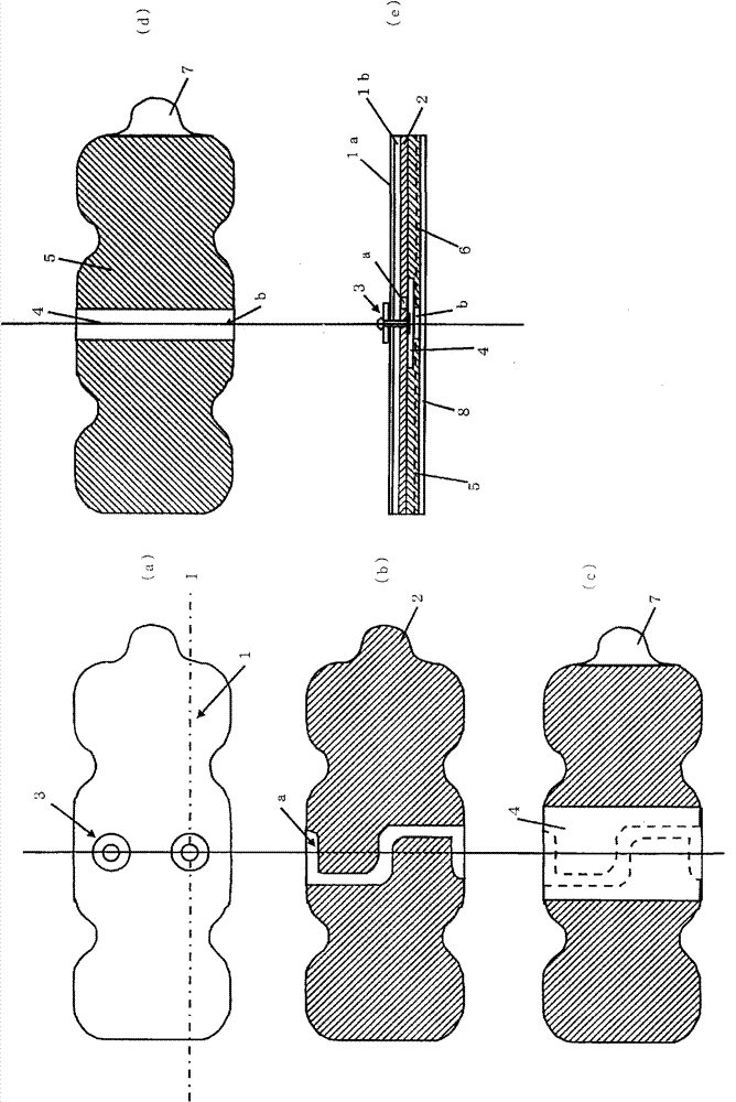
[0130] image 3 (a)-(e) shows the schematic diagram of the 2-terminal type antistatic tool of Example 2. image 3 (a) is the top view schematic diagram of the antistatic appliance of embodiment 2, image 3 (b) is a figure which shows the arrangement|positioning of the electroconductive layer of the antistatic tool of Example 1. image 3 The hatched portion in (b) is a conductive layer, and there is an S-shaped portion a where no conductive layer is formed near the center. image 3 (c) The figure which shows the state which laminated|stacked the covering layer and the non-adhesive layer. image 3 (d) The figure which shows the state which laminated|stacked the electroconductive adhesive layer. image 3 In (d), there exists a part b in which the electroconductive adhesive layer is not formed. image 3(e) is a schematic cross-sectional view of the I-I line of the antistatic appliance in embodiment 2. The terminal part of the antistatic appliance of embodiment 2 has figure ...
PUM
 Abstract
Description
Claims
Application Information


