Fabricating method of touch circuit two-sided graph structure

A technology for touch circuits and graphic structures, which is applied in the photoengraving process of circuits and pattern surfaces, electrical components, etc., can solve the problems of consuming process time and material costs, and insurmountable problems.

Inactive Publication Date: 2010-06-09
TRENDON TOUCH TECHNOLOGY CORPORATION
View PDF4 Cites 30 Cited by
  • Summary
  • Abstract
  • Description
  • Claims
  • Application Information

AI Technical Summary

Problems solved by technology

[0004] However, in the manufacturing method of the double-sided graphic structure of the above-mentioned traditional touch circuit, the yellow light process must be repeated many times, including multiple contact and removal of the photoresist layer and protective layer, and the steps of developing and etching must be repeated multiple times. And after completing at least two yellowing processes of the upper and lower conductive films, it is still necessary to carry out another yellowing process for the metal circuit layer, resulting in the problem of consuming process man-hours and material costs.
In addition, optoelectronic products involving the above-mentioned yellow light process in the prior art can be found in US Patent No. 20070269936, No. 20020048730, No. 6037005 and Chinese Patent No. CN1549004; however, none of them involve the application of double-sided etching , so it is obviously impossible to overcome the above-mentioned problem of repeating the yellow light process many times, and it needs to be improved urgently

Method used


Image

  • Fabricating method of touch circuit two-sided graph structure
  • Fabricating method of touch circuit two-sided graph structure
  • Fabricating method of touch circuit two-sided graph structure

Examples


Embodiment Construction

[0091] The effects that can be produced by the manufacturing method of the double-sided graphic structure of the touch circuit of the present invention are described in detail as follows with preferred embodiments in conjunction with the accompanying drawings:

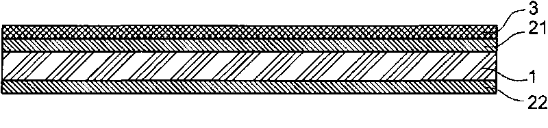
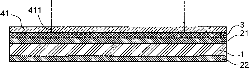
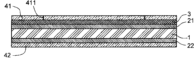
[0092] see figure 1 , revealing a cross-sectional view of an embodiment of the present invention, illustrating the method for manufacturing the double-sided graphic structure of the touch circuit of the present invention, including the following steps:

[0093] (1) A transparent substrate 1 is placed in a sputtering equipment, and a first conductive substrate layer 21 is formed on the top surface of the substrate 1 by vacuum sputtering (such as figure 1 As shown), a second conductive substrate layer 22 is formed on the bottom surface of the substrate 1 at the same time; 22 can be made of transparent conductive material, and the transparent conductive material can be indium tin oxide (ITO) or other conductive materials...


PUM


Abstract

The invention relates to a fabricating method of a touch circuit two-sided graph structure, which comprises the steps of: providing a substrate with a first conducting base material layer and a second conducting base material layer distributed on two sides of the substrate, contacting with a shielding layer for shielding ultraviolet on the top face of the first conducting base material layer; contacting with a first light resistance layer on the top face of the shielding layer, contacting with a second light resistance layer on the bottom face of the second conducting base material layer; exposing the first light resistance layer and the second light resistance layer, shielding ultraviolet on two sides of the substrate through the shielding layer; developing two sides of the substrate to ensure that the first conducting base material layer and the second conducting base material layer respectively expose regions to be etched; and etching the exposed regions of the first conducting base material layer and the second conducting base material layer to ensure that the first conducting base material layer forms a first conducting film of the touch circuit and the second conducting base material layer forms a second conducting film of the touch circuit. Therefore, the invention can simultaneously expose, develop and etch two sides of the substrate so as to simplify the layout procedure of the touch circuit.

Description

technical field [0001] The invention relates to a method for manufacturing a touch circuit, in particular to a method for manufacturing a graphic structure of a touch circuit formed by arranging on both sides of a transparent substrate by means of sputtering, exposure, development, etching and the like. Background technique [0002] Touch Panel, for example, is more common in the market, usually resistive and capacitive touch panels. Among them, the capacitive touch panel has a double-sided graphic structure of a touch circuit. It uses exposure, development, etching and other yellow light processes to stack transparent conductive materials (Indium Tin Oxide, ITO) on a glass one by one. The substrate (Glass Substrate) is formed on both sides, including an upper conductive film arranged on the top surface of the glass substrate, and a lower conductive film arranged on the bottom surface of the glass substrate, and a metal circuit layer is arranged on the top surface of the gla...

Claims


Application Information

Patent Timeline
Patent Type & Authority Applications(China)
IPC IPC(8): G02F1/133G03F7/00G06F3/041H01L21/00
Inventor 刘振宇王净亦刘正平李禄兴
Owner TRENDON TOUCH TECHNOLOGY CORPORATION
Why Eureka
Try Eureka