Liquid crystal panel

A technology of liquid crystal panels and transistors, applied in nonlinear optics, instruments, optics, etc., can solve problems affecting the pixel voltage of liquid crystal capacitor C1c2, affecting display quality and stability, and drifting, so as to reduce the feedthrough effect, reduce the impact, The effect of reducing the number

Inactive Publication Date: 2013-11-06
INNOLUX CORP
View PDF2 Cites 0 Cited by
  • Summary
  • Abstract
  • Description
  • Claims
  • Application Information

AI Technical Summary

Problems solved by technology

Therefore, during the driving process, the pixel voltages on the pixel unit 111 and the pixel unit 121 will have different voltage changes due to the scanning signal, which will affect the quality and stability of the display.
[0017] In addition, when the even scan line SE i When disabled, the odd scan line SO i It will be in a floating state, because there are many circuit lines or capacitors near the gate of the transistor M111, which will cause the gate voltage of the transistor M111 to drift to the common voltage Vcom due to these electrical couplings and affect the liquid crystal capacitance C1c2 pixel voltage on

Method used


Image

  • Liquid crystal panel
  • Liquid crystal panel
  • Liquid crystal panel

Examples


no. 1 example

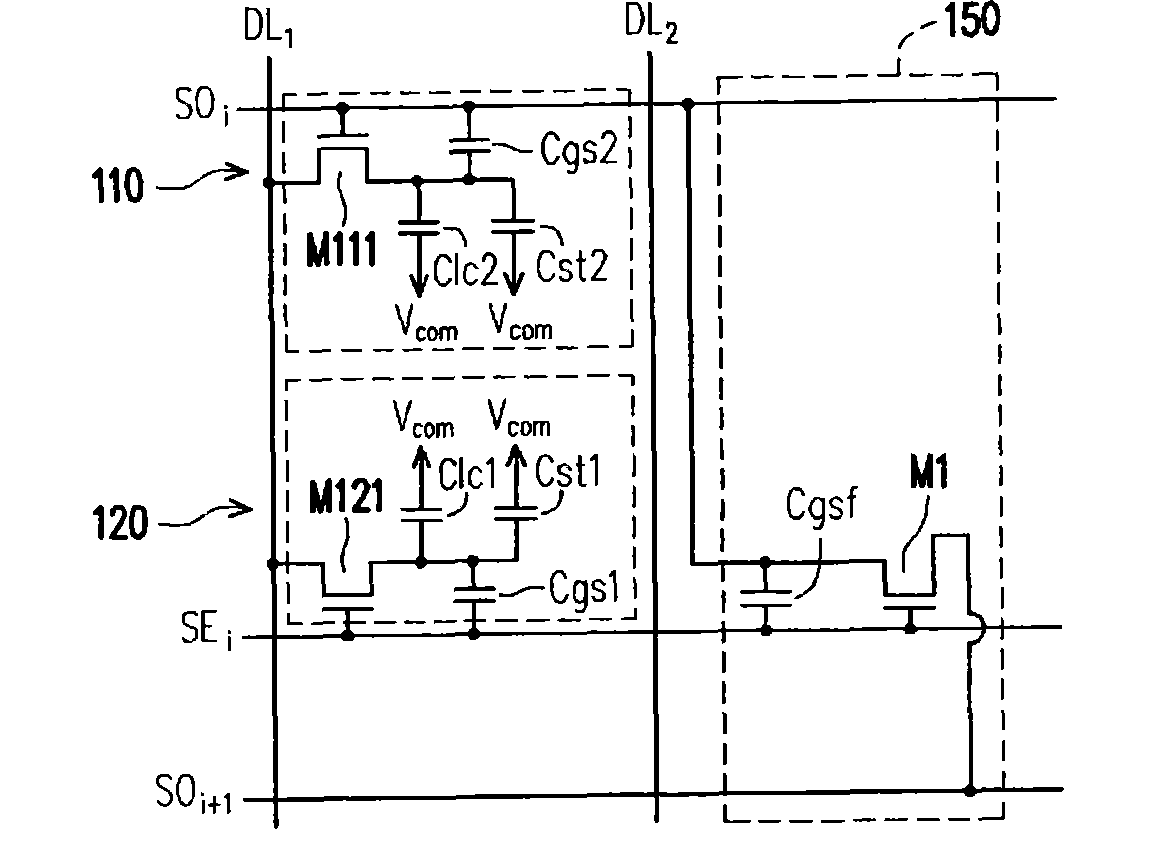
[0085] Also refer to Figure 1 to Figure 3 , in order to reduce the feedthrough voltage ΔV2 of the pixel unit 111, this embodiment i Connect the capacitor Cst, such as Figure 4 as shown, Figure 4 It is a partial circuit schematic diagram of the liquid crystal panel according to the first embodiment of the present invention. Among them, the capacitor Cst and the odd scan line SO i The pixel units 111 above are connected in parallel to increase the capacitance value after the parallel connection. Referring to the above formula (2), after adding the capacitor Cst, (Cgs+n×CX) in the formula (2) becomes (Cgs+n×CX+Cst), that is, its value becomes larger, so the feedthrough voltage ΔV2 will be It will decrease and be closer to the feedthrough voltage ΔV1. Since the capacitor Cst is connected in parallel to the odd scan line SO i All pixel units (such as 112) on the above, so the capacitor Cst also has the function of reducing the odd scan line SO i The effect of the feed-thr...

no. 2 example

[0089] In addition to reducing the odd scan line SO by adding a capacitor Cst i with even scan line SE i In addition to the difference between the voltages ΔV1 and ΔV2 , this embodiment also proposes a method for reducing the difference between the pull-back voltages ΔV1 and ΔV2 by adjusting the driving waveform of the scan signal.

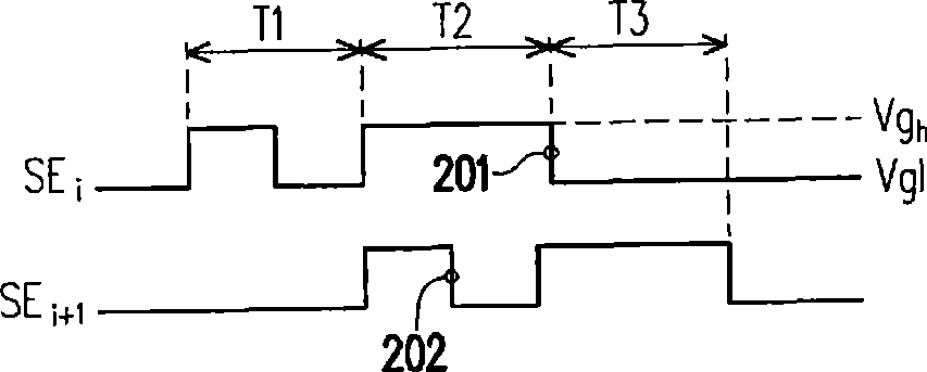
[0090] Also refer to Figure 6 and figure 1 , Figure 6 It is a scanning signal waveform diagram according to the second embodiment of the present invention, which is suitable for driving such as figure 1 LCD panel. Wherein, in the second period T2, the even scan line SE i The voltage value of the enable voltage 620 is Vgh2, and the even scanning line SE i+1 The voltage value of the enabling voltage 610 is Vgh1, wherein Vgh2 is greater than Vgh1. Vgl is even scan line SE i+1 or even scan line SE i The voltage value when disabled (or called logic low level). Due to the even scan line SE i 、SE i+1 The waveform of the scanning signal chan...

no. 3 example

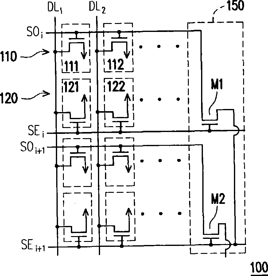
[0096] Figure 7 It is a schematic circuit diagram of a liquid crystal panel according to a third embodiment of the present invention, in Figure 7 , the local circuit 700 in the liquid crystal panel includes a plurality of data lines (such as DL 1 、DL 2 ), control line SC i , odd scan line SO i and the even scan line SE i , where i is the index value of the scan line, if the liquid crystal panel includes N scan lines, then 0i As an example, it corresponds to the odd scan line SO i with even scan line SE i , odd scan line SO i used to scan the odd pixel column 710, while the even scan line SE i It is used to scan the even pixel column 720 , wherein the odd pixel column 710 and the even pixel column 720 respectively include a plurality of pixel units (such as 711 , 712 , 721 , 722 ). The structure of the pixel unit is the same as the known technology, that is, it has structures such as liquid crystal capacitors, storage capacitors (not shown), and transistors. Different...


PUM


Abstract

The invention discloses a liquid crystal panel, which is provided with N scanning lines and N pixel columns. The liquid crystal panel comprises the ith scanning line, the (i+1)th scanning line, the (i+3)th scanning line, a first transistor and a first capacitor, wherein the ith scanning line is used for scanning the ith pixel column; the (i+1)th scanning line is used for scanning the (i+1)th pixel column; the (i+3)th scanning line is used for scanning the (i+3)th pixel column; and the ith pixel column is adjacent to the (i+1)th pixel column. The first transistor is coupled between the ith scanning line and the (i+3)th scanning line, and a gate of the first transistor is coupled with the (i+1)th scanning line. The first capacitor is coupled between the ith scanning line and the common end to reduce the feed-through effect on the ith scanning line, wherein N and i are positive integers, and i is less than or equal to N-3.

Description

technical field [0001] The present invention relates to a liquid crystal panel with pixel level multiplexing (Pixel Level Multiplexing, PLM) architecture, and in particular to a liquid crystal panel that can reduce the number of required gate drivers. Background technique [0002] There are various types of flat panel displays (FPDs), such as liquid crystal displays (LCDs), organic electroluminescent displays (OLEDs), and plasma displays (PDPs). However, no matter what kind of flat panel display it is, the structure of the display panel is similar, that is, the substrate is provided with criss-cross scan lines and data lines, and each scan line is connected to the data line. One pixel (pixel) is arranged at the intersection of the lines. The pixels receive scan signals through the scan lines to determine whether to be enabled or turned on, and receive data signals through the data lines to display images when they are turned on. [0003] The higher the resolution of the li...

Claims


Application Information

Patent Timeline
Patent Type & Authority Patents(China)
IPC IPC(8): G02F1/1362G09G3/36
Inventor 杨咏舜
Owner INNOLUX CORP
Why Eureka
Try Eureka