Liquid crystal display panel and liquid crystal display device

A technology for liquid crystal display panels and substrates, which is used in static indicators, nonlinear optics, instruments, etc., can solve the problems of low contrast, high cost, and complicated process of liquid crystal display panels, and achieves the improvement of contrast, simplification of the process, and increased contrast. Effect

Active Publication Date: 2010-06-16
KUSN INFOVISION OPTOELECTRONICS
View PDF0 Cites 11 Cited by
  • Summary
  • Abstract
  • Description
  • Claims
  • Application Information

AI Technical Summary

Problems solved by technology

However, disposing the protrusions 50 on the color filter substrate 80 will generally cause light leakage and reduce the contrast of the liquid crystal display panel. Moreover, it needs to add a photolithography process on the color filter substrate, which makes the manufacturing process complicated and the cost is high.

Method used


Image

  • Liquid crystal display panel and liquid crystal display device
  • Liquid crystal display panel and liquid crystal display device
  • Liquid crystal display panel and liquid crystal display device

Examples


no. 1 example

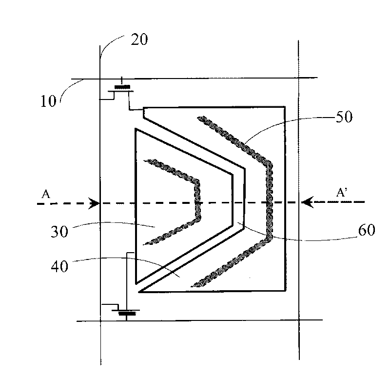
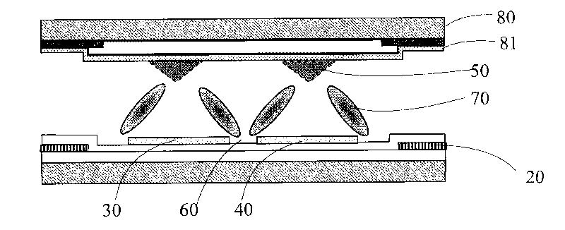
[0037] Figure 3 to Figure 5 Shown is a liquid crystal display panel according to a first embodiment of the present invention. image 3 It is a schematic structural diagram of a single pixel of the liquid crystal display panel of the first embodiment, Figure 4 is along image 3 The sectional view of the line B-B' in the middle, Figure 5 It is a partial structure diagram of the liquid crystal display panel of the first embodiment of the present invention. For highlighting the invention point of the present invention, image 3 Only a single pixel area is shown in , which should actually include such as Figure 5 An array of multiple pixel regions is shown in .

[0038] The liquid crystal display panel in this embodiment is a novel multi-region vertical alignment type liquid crystal display panel, which includes: a first substrate 10, a second substrate 20 opposite to the first substrate 10, and a substrate sandwiched between the first substrate 10 and the liquid crystal ...

no. 2 example

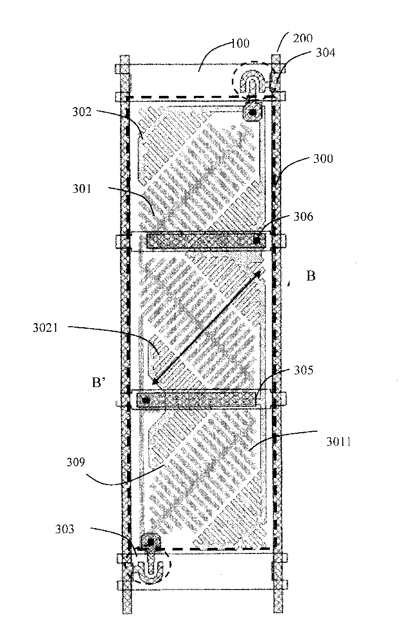
[0061] Image 6 It is a partial structural schematic diagram of the liquid crystal display panel according to the second embodiment of the present invention.

[0062] Similarly, the pixel area of ​​the liquid crystal display panel according to the second embodiment of the present invention also has the first sub-pixel electrode 301 and the second sub-pixel electrode 302 respectively in the shape of fishbone, and the first sub-pixel electrode 301 and the second sub-pixel The electrodes 302 have a nested structure, wherein the first sub-pixel electrode 301 has at least one nesting region 3011 extending into the second sub-pixel electrode 302, and the second sub-pixel electrode 302 has at least one nesting region 3011 extending into the first sub-pixel Nesting region 3021 within electrode 301 . In addition, when the liquid crystal display panel is working, since the first sub-pixel electrode 301 and the second sub-pixel electrode 302 nested therein have opposite polarities, the ...

no. 3 example

[0066] Figure 7 It is a partial structural schematic diagram of the liquid crystal display panel according to the third embodiment of the present invention.

[0067] Similarly, the pixel area of ​​the liquid crystal display panel in the third embodiment of the present invention also has the first sub-pixel electrode 301 and the second sub-pixel electrode 302 respectively in the shape of fishbone, and the first sub-pixel electrode 301 and the second sub-pixel The electrodes 302 have a nested structure, wherein the first sub-pixel electrode 301 has at least one nesting region 3011 extending into the second sub-pixel electrode 302, and the second sub-pixel electrode 302 has at least one nesting region 3011 extending into the first sub-pixel Nesting region 3021 within electrode 301 . In addition, when the liquid crystal display panel is working, since the first sub-pixel electrode 301 and the second sub-pixel electrode 302 nested therein have opposite polarities, the first sub-p...


PUM


Abstract

The invention provides a liquid crystal display panel and a liquid crystal display device, comprising a first substrate, a second substrate and a liquid crystal layer, wherein the first substrate and the second substrate are arranged opposite to each other, and the liquid crystal layer is clamped between two substrates, the first substrate comprises a plurality of pixel regions defined by a plurality of scanning lines and a plurality of data lines, and the pixel regions at least comprise a first sub-pixel electrode and a second sub-pixel electrode, a first film transistor and a second film transistor. The first sub-pixel electrode and the second sub-pixel electrode are electrically isolated from each other and the polarities of the first sub-pixel electrode and the second sub-pixel electrode are opposite when the liquid crystal display panel operates; the first sub-pixel electrode and the second sub-pixel electrode are nested with each other, wherein the first sub-pixel electrode is provided with at least one nesting region extending into the second sub-pixel electrode, and the second sub-pixel electrode is provided with at least one nesting region extending into the first sub-pixel electrode. The liquid crystal display panel saves photoetching process of a projection structure and a gap in the process of manufacturing a color filter substrate, simplifies the process, reduces the cost and improves the contrast ratio at the same time.

Description

technical field [0001] The present invention relates to the field of thin film transistor liquid crystal display (Thin Film Transistor Liquid Crystal Display, TFT-LCD), in particular to a multi-region vertical alignment (Vertical Alignment, VA) liquid crystal display panel and a liquid crystal display device thereof. Background technique [0002] As a flat panel display, liquid crystal display (LCD) has many advantages such as clear and accurate image, thin thickness, light weight, no radiation, low energy consumption and low working voltage, and has been widely used in various fields. Generally, a liquid crystal display has two substrates containing electrodes, and a liquid crystal layer arranged between the two substrates. The electric field intensity applied to the liquid crystal layer is controlled by the electrodes on the two substrates to control the deflection of the liquid crystal molecules, thereby adjusting the intensity of the incident light. Transmittance, in ord...

Claims


Application Information

Patent Timeline
Patent Type & Authority Applications(China)
IPC IPC(8): G02F1/1362G02F1/1368G02F1/133
Inventor 乔艳冰钟德镇简廷宪
Owner KUSN INFOVISION OPTOELECTRONICS
Why Eureka
Try Eureka