
Complementary metal oxide semiconductor transistor device and manufacturing method thereof

A technology of oxide semiconductors and transistors, applied in semiconductor/solid-state device manufacturing, semiconductor devices, transistors, etc., can solve problems such as device performance degradation, achieve the effects of alleviating the difficulty of etching, simplifying the manufacturing process, and expanding the scope of research

Active Publication Date: 2011-06-15
SOI MICRO CO LTD
View PDF0 Cites 0 Cited by
  • Summary
  • Abstract
  • Description
  • Claims
  • Application Information

AI Technical Summary

Problems solved by technology

A major challenge in using high-k dielectrics in CMOS devices is high threshold voltage, which can lead to degraded device performance

Method used


Image

  • Complementary metal oxide semiconductor transistor device and manufacturing method thereof
  • Complementary metal oxide semiconductor transistor device and manufacturing method thereof
  • Complementary metal oxide semiconductor transistor device and manufacturing method thereof

Examples


Embodiment Construction

[0059] In order to make the object, technical solution and advantages of the present invention clearer, the present invention will be described in further detail below in conjunction with specific embodiments and with reference to the accompanying drawings.

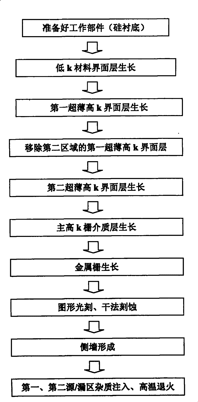
[0060] Such as figure 1 as shown, figure 1 It is a flow chart of the manufacturing method of the CMOS transistor device provided by the present invention, and the method includes:

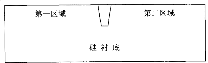
[0061] Step 101: providing a silicon substrate, the silicon substrate includes a first region and a second region;

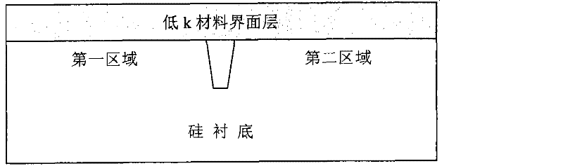
[0062] Step 102: forming a low-k material interface layer on the silicon substrate;

[0063] Step 103: forming a first ultra-thin high-k interface layer structure on the low-k material interface layer;

[0064] Step 104: removing the first ultra-thin high-k interface layer structure on the low-k material interface layer on the second region;

[0065] Step 105: forming a second ultra-thin high-k interface layer structure on t...


PUM


Abstract

The invention discloses a complementary metal oxide semiconductor (CMOS) transistor device and a manufacturing method thereof. The CMOS transistor device comprises a silicon substrate, a first transistor and a second transistor. The CMOS transistor device with a structure of a main high k-grid dielectric layer and an ultrathin high k interface layer structure and the manufacturing method thereof provided by the invention effectively solve the problem of high threshold voltage caused by using high k dielectric in the CMOS transistor devices of the technical generation below 32 nanometers. Due to the adoption of the CMOS transistor device structure, the threshold voltage of the CMOS transistor device can be effectively controlled by adding a layer of the ultrathin high k interface layer structure under the main high k layer.

Description

technical field [0001] The invention relates to the technical field of semiconductors, in particular to a complementary metal oxide semiconductor (Complimentary Metal Oxide Semiconductor, CMOS) transistor device and a manufacturing method thereof. Background technique [0002] Since the first integrated circuit came out in 1958, microelectronics technology has developed very rapidly and has become the basis of the entire information industry. The core of microelectronics technology - CMOS technology (invented in 1963) has become a supporting technology in modern electronic products. For decades, logic chipmakers have used silicon dioxide (SiO 2 ) as the gate dielectric and heavily doped polysilicon (poly-Si) as the gate electrode material. This combination continued into the 90nm technology generation. SiO in CMOS transistors as feature sizes continue to shrink 2 The gate dielectric is approaching its limit. For example, at 65nm process, SiO 2 The thickness of the gate...

Claims


Application Information

Patent Timeline
Patent Type & Authority Patents(China)
IPC IPC(8): H01L27/092H01L29/78H01L29/51H01L21/8238
Inventor 王文武陈世杰
Owner SOI MICRO CO LTD
Learn More