
SONOS flash memory unit and manufacturing method thereof

A technology of flash memory unit and manufacturing method, which is applied in semiconductor/solid-state device manufacturing, electrical components, electric solid-state devices, etc., can solve problems such as increasing process complexity, reduce short-channel effects, overcome programming difficulties, and improve programming efficiency effect

Active Publication Date: 2010-06-16
SHANGHAI HUAHONG GRACE SEMICON MFG CORP
View PDF0 Cites 11 Cited by
  • Summary
  • Abstract
  • Description
  • Claims
  • Application Information

AI Technical Summary

Problems solved by technology

Deep N-well increases process complexity

Method used


Image

  • SONOS flash memory unit and manufacturing method thereof
  • SONOS flash memory unit and manufacturing method thereof
  • SONOS flash memory unit and manufacturing method thereof

Examples


Embodiment Construction

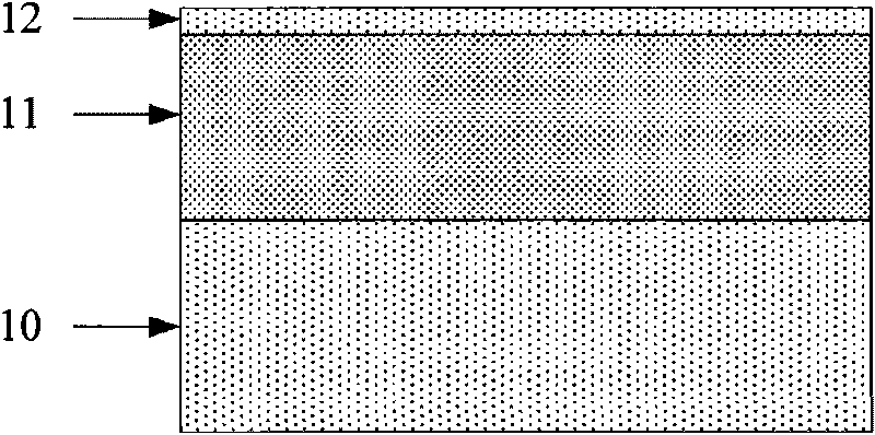
[0032] Step 1, see Figure 1a , N-type impurities are implanted on the P-type silicon substrate 10 by ion implantation process to form an N well 11 . Commonly used N-type impurities are phosphorus, arsenic, antimony, etc. Next, P-type impurities are implanted on the N well 11 by using an ion implantation process to form a P-type buried trench 12 . Commonly used P-type impurities include boron and the like.

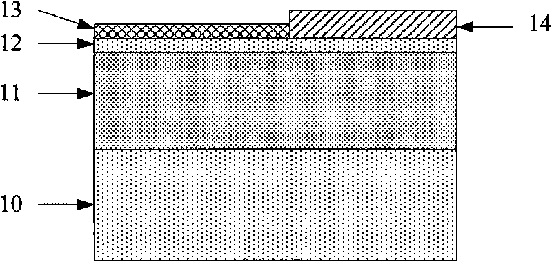
[0033] Step 2, see Figure 1b 1. Deposit a layer of ONO (silicon oxide / silicon nitride / silicon oxide) dielectric 13 and a layer of silicon oxide 14 on the surface of the silicon wafer, which are respectively used for the gate dielectric layer and the gate oxide layer of the SONOS device. The ONO dielectric 13 and the silicon oxide 14 are arranged horizontally instead of vertically.

[0034] For example, a layer of silicon oxide 14 can be completely deposited on the surface of the silicon wafer first, then coated with photoresist, exposed and developed to expose the etc...


PUM


Abstract

The invention discloses an SONOS flash memory unit and a manufacturing method thereof, wherein an SONOS component and a selected transistor both adopt enhanced PMOS components, therefore, the substrate bias of the components can be realized without a deep N-well process. A P-type buried channel on the surface of an N-well can provide a great deal of cavities for the programming of the SONOS component, thereby greatly improving the programming efficiency and overcoming the defects of large effective quality and difficult programming of the cavities. The P-type SONOS component can obtain a programming and erasing threshold voltage which is more symmetrical than that of an N-type SONOS component; furthermore, the invention ensures that the drain electrode implantation volume is larger than that of a source electrode, increases the effective channel length and creates conditions for shortening the size of the components by fully utilizing the characteristic of small grid spacing between the two components of the flash memory unit and adopting source-drain ion implantation with large angle and light dope; and finally, the invention further reduces the short channel effect by carrying out bag-shaped ion implantation on the two components of the flash memory unit.

Description

technical field [0001] The invention relates to a semiconductor integrated circuit structure, in particular to a SONOS flash memory unit. Background technique [0002] SONOS (Silicon-Oxide-Nitride-Oxide-Silicon, Silicon-Oxide-Nitride-Oxide-Silicon) flash memory is through the ONO (Silicon Oxide-Silicon Nitride-Silicon Oxide, Oxide-Nitride-Oxide) dielectric layer Silicon nitride stores electrons or holes to realize the erasing and writing function of flash memory. Carriers (electrons or holes) migrate through tunnel current by applying a bias voltage between the gate, drain and channel. [0003] A SONOS flash memory cell is composed of a SONOS device plus a select transistor connected in series. During the erasing and writing process of the SONOS flash memory unit, the source of the SONOS device, the source and the drain of the selection transistor are all in a floating state. In the process of "reading" the SONOS flash memory unit, the selection transistor is in the condu...

Claims


Application Information

Patent Timeline
Patent Type & Authority Applications(China)
IPC IPC(8): H01L27/115H01L21/8247H10B69/00
Inventor 钱文生
Owner SHANGHAI HUAHONG GRACE SEMICON MFG CORP
Learn More