Multispectral sensitization device and manufacturing method thereof

A photosensitive device and multi-spectral technology, which is applied in semiconductor/solid-state device manufacturing, electrical components, radiation control devices, etc., can solve the problems of reduced sensitivity of filter films, lower space and energy usage efficiency than multi-layer, and inability to respond to different scenes Light and other issues, to achieve low-cost effects

Inactive Publication Date: 2010-06-16
BOLY MEDIA COMM SHENZHEN
View PDF5 Cites 33 Cited by
  • Summary
  • Abstract
  • Description
  • Claims
  • Application Information

AI Technical Summary

Problems solved by technology

[0005] As mentioned above, there are three common difficulties in realizing the filter film technology by composite color (green, yellow, peach and green) patterns, Bayeux patterns, or honeycomb patterns: The first difficulty is the reduction in sensitivity caused by the filter film (relative to black and white sensor chip)
The second difficulty is the reduction in effective sharpness (or resolution) due to color interpolation
For a single-layer photosensitive chip, it has encountered a bottleneck in sensitivity, and its space and energy usage efficiency is not as good as that of a multi-layer chip.
For multi-layer (two-layer or three-layer) photosensitive chips, the processing complexity is naturally much more difficult.
Another function that the existing photosensitive chip technology does not have is that they cannot simultaneously sense the light corresponding to different scenes from the front and back directions.

Method used


Image

  • Multispectral sensitization device and manufacturing method thereof
  • Multispectral sensitization device and manufacturing method thereof
  • Multispectral sensitization device and manufacturing method thereof

Examples


Embodiment Construction

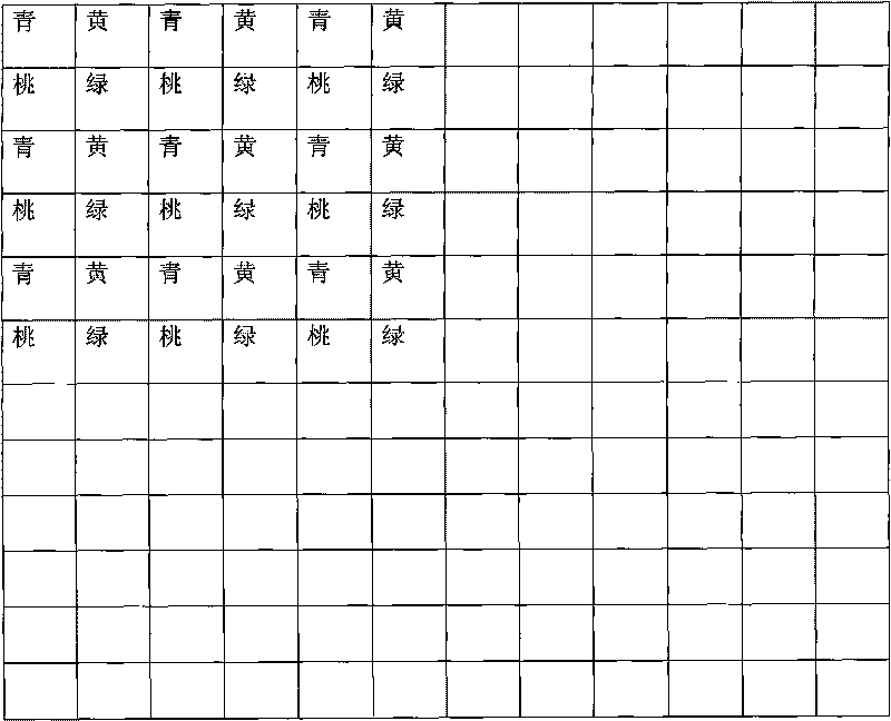
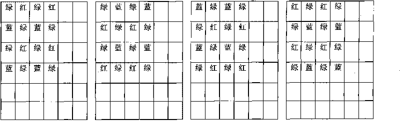
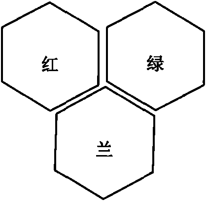
[0075] The multi-spectrum photosensitive device, manufacturing method and photosensitive system of the present invention are mainly provided with photosensitive pixel groups on each surface of the base layer having one or more surfaces, so as to obtain scenes in different directions at the same time. It should be understood that the shape of the base layer is not limited, for example, it may be rectangular, circular pie, hexahedron and so on. When the base layer is opaque, there is more selectivity in setting its shape. When the base layer is transparent, it is preferable to use a two-sided thin cuboid and hexahedron to facilitate the acquisition of corresponding pixel positions on the opposite surfaces.

[0076]The present invention will be described below by taking the base layer as a planar body (cuboid with extremely thin thickness) as an example. At this time, the photosensitive device of the present invention realizes bidirectional photosensitive, that is, photosensitiv...


PUM


Abstract

The invention relates to a multispectral sensitization device and a manufacturing method thereof. The device comprises at least one non-transparent basement layer, each basement layer is composed of at least two surfaces, each surface is provided with sensitization pixel groups which are used for inducing light of optional spectrum coming from the positive direction of the surfaces where the sensitization pixel groups are located; or the device comprises at least one transparent basement layer, each basement layer is composed of at least two surfaces, each surface is provided with sensitization pixel groups which are used for inducing light of optional spectrum coming from the positive side or the reverse side of the surfaces where the sensitization pixel groups are located. In the invention, bidirectional sensitization can be realized through a same device, different scenes in two different directions can be induced; in addition, the device can be used for unidirectional sensitization to improve properties of the sensitization device.

Description

technical field [0001] The invention relates to a multi-spectrum photosensitive device and a manufacturing method thereof. More precisely, the present invention relates to a photosensitive device for full-color images capable of simultaneously sensing multiple spectrums (such as visible light and infrared light) and a fabrication method thereof. Here, panchromatic refers to the entire spectrum of interest. For ordinary (visible light) photosensitive devices, panchromatic refers to covering the entire visible spectrum of red, green, blue and white. For photosensitive devices that combine infrared and color, panchromatic refers to the visible spectrum and the infrared spectrum. The invention is applicable to multispectral photosensitive devices including black and white and color images. Background technique [0002] The traditional technology of designing and manufacturing color image photosensitive chips (or devices) either uses single-layer photosensitive pixels or three...

Claims


Application Information

Patent Timeline
Patent Type & Authority Applications(China)
IPC IPC(8): H01L27/146H01L21/82
Inventor 胡笑平
Owner BOLY MEDIA COMM SHENZHEN
Why Eureka
Try Eureka