
A field effect transistor device using carbon nanotubes as electrodes and its preparation method

A field effect transistor and carbon nanotube technology is applied in the field of field effect transistor devices and their preparation to achieve the effects of high response sensitivity and high application value

Inactive Publication Date: 2011-12-28
PEKING UNIV
View PDF0 Cites 2 Cited by
  • Summary
  • Abstract
  • Description
  • Claims
  • Application Information

AI Technical Summary

Problems solved by technology

However, so far, there are few reports on single-walled carbon nanotubes as one-dimensional electrode materials and on the electrical properties of semiconducting molecular materials.

Method used


Image

  • A field effect transistor device using carbon nanotubes as electrodes and its preparation method
  • A field effect transistor device using carbon nanotubes as electrodes and its preparation method
  • A field effect transistor device using carbon nanotubes as electrodes and its preparation method

Examples


Embodiment 1

[0030] Example 1. Preparation of carbon nanotube transistor device

[0031] The preparation method of the carbon nanotube transistor device sequentially includes the following steps:

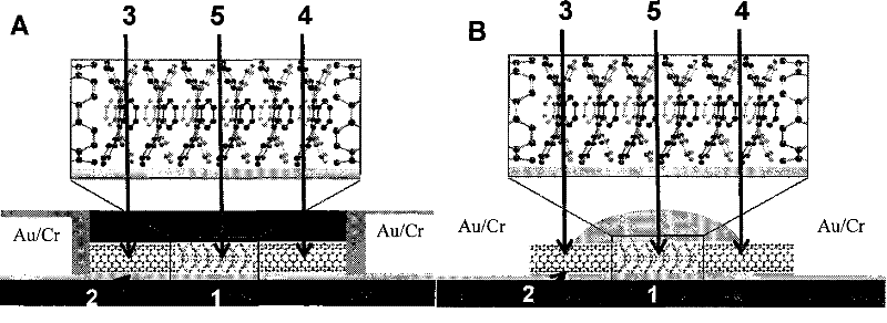
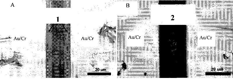
[0032] 1) Mesoporous SiO doped with CoMo 2 The particles act as a catalyst, and the catalyst is evenly distributed on the SiO on the surface of the heavily doped silicon substrate 2 Above the layer; the SiO 2 The layer is grown on the silicon wafer by thermal evaporation method with a thickness of 300nm; ethanol is used as the carbon source, and the CVD method is used in SiO 2 A single-walled carbon nanotube layer is obtained on the layer. The single-walled carbon nanotube layer is located in the center of the silicon substrate.

[0033] Afterwards, a metal mask is covered on the single-walled carbon nanotube layer, and a Cr layer and an Au layer are sequentially obtained by a thermal evaporation method, and Au / Cr is used as the source region and the drain region of the carbon nanotube transistor devic...

Embodiment 2

[0042] Example 2. Preparation of carbon nanotube transistor device

[0043] The preparation method of the carbon nanotube transistor device sequentially includes the following steps:

[0044] 1) Mesoporous SiO doped with CoMo 2 The particles act as a catalyst, and the catalyst is evenly distributed on the SiO on the surface of the heavily doped silicon substrate 2 Above the layer; the SiO 2 The layer is grown on the silicon wafer by thermal evaporation method with a thickness of 300nm; ethanol is used as the carbon source, and the CVD method is used in SiO 2 A single-walled carbon nanotube layer is obtained on the layer. The single-walled carbon nanotube layer is located in the center of the silicon substrate.

[0045] Afterwards, a metal mask is covered on the single-walled carbon nanotube layer, and a Cr layer and an Au layer are sequentially obtained by a thermal evaporation method, and Au / Cr is used as the source region and the drain region of the carbon nanotube transistor devic...

Embodiment 3

[0054] Example 3. Preparation of carbon nanotube transistor device

[0055] 1) Mesoporous SiO doped with CoMo 2 The particles act as a catalyst, and the catalyst is evenly distributed on the SiO on the surface of the heavily doped silicon substrate 2 Above the layer; the SiO 2 The layer is grown on the silicon wafer by thermal evaporation method with a thickness of 300nm; ethanol is used as the carbon source, and the CVD method is used in SiO 2 A single-walled carbon nanotube layer is obtained on the layer. The single-walled carbon nanotube layer is located in the center of the silicon substrate.

[0056] Afterwards, a metal mask is covered on the single-walled carbon nanotube layer, and a Cr layer and an Au layer are sequentially obtained by a thermal evaporation method, and Au / Cr is used as the source region and the drain region of the carbon nanotube transistor device. The distance between the two electrodes is 20 μm, the thickness of the Cr layer is 5 nm, and the thickness of t...


PUM

PropertyMeasurementUnit
thicknessaaaaaaaaaa
widthaaaaaaaaaa
widthaaaaaaaaaa

Abstract

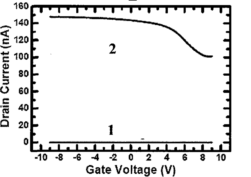
The invention provides a field effect transistor device using carbon nanotubes as electrodes and a preparation method thereof. In the device, the materials constituting the source region and the drain region are at least one single-wall carbon nanotube, and the materials constituting the channel region are various organic semiconductor molecules. The preparation method provided by the invention introduces functionalized molecules into functional molecular transistor devices by combining a top-down device manufacturing process and a bottom-up molecular self-assembly method. By using one-dimensional ballistic single-walled carbon nanotubes as point contacts and introducing hexabenzocoronene compounds with self-assembly properties, high-performance nanometer field-effect transistors can be obtained, which have high response sensitivity to various external stimuli. The carbon nanotube transistor device provided by the invention has high application value in ultrasensitive environmental stimulus response, ultrasensitive solar stimulus response device and the like. The device will play a vital role in promoting the development of ultra-micro optoelectronic devices at various scales at the molecular level.

Description

Technical field [0001] The invention relates to a transistor device and a preparation method thereof, in particular to a field effect transistor device using carbon nanotubes as electrodes and a preparation method thereof. Background technique [0002] The preparation method of molecular transport junction is of great significance to promote the development of molecular electronics. The electrical properties of single or multiple molecules can be obtained through molecular transport junction. In the field of molecular electronics, the biggest problem is still the construction, measurement, characterization, and theoretical research of the current-voltage response of electronic circuits, and molecular systems play a vital role as conductive elements in electronic circuits. Single-walled carbon nanotubes are quasi-one-dimensional ballistic conductors with molecular dimensions, suitable for nanoscale processing, and have unique photoelectric properties. It has been confirmed that s...

Claims


Application Information

Patent Timeline
Patent Type & Authority Patents(China)
IPC IPC(8): H01L51/05H01L51/30H01L51/40
Inventor 郭雪峰
Owner PEKING UNIV
Learn More