Signal processor and signal processing method
A signal processing device and a technology for testing signals, applied in DC level restoration devices/bias distortion correction, digital transmission systems, electrical components, etc., can solve problems such as performance degradation
- Summary
- Abstract
- Description
- Claims
- Application Information
AI Technical Summary
Problems solved by technology
Method used
Image


Examples
no. 1 approach
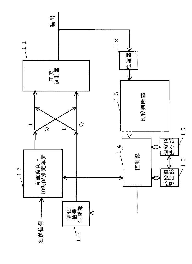
[0113] figure 1 It is a diagram showing the configuration of the signal processing device according to the first embodiment of the present invention. refer to figure 1 It can be seen that the signal processing device according to one embodiment of the present invention includes a test signal generation unit 10, a DC offset IQ mismatch estimation unit 17, a quadrature modulator 11, a wave detector 12, a comparison and judgment unit 13, and a control unit 14. , an adjustment value storage unit 15 , and a compensation value derivation unit 16 . Briefly speaking, each of the above-mentioned parts executes the following processes and operations. The test signal generator 10 generates a first test signal (I 1 , Q 1 ) (wherein, in (I, Q), I represents the in-phase component signal, Q represents the quadrature component signal) and the second test signal (I 2 , Q 2 ) and supply them to the quadrature modulator 11. Quadrature modulator 11 to the first test signal (I 1 , Q 1 ...
no. 2 approach
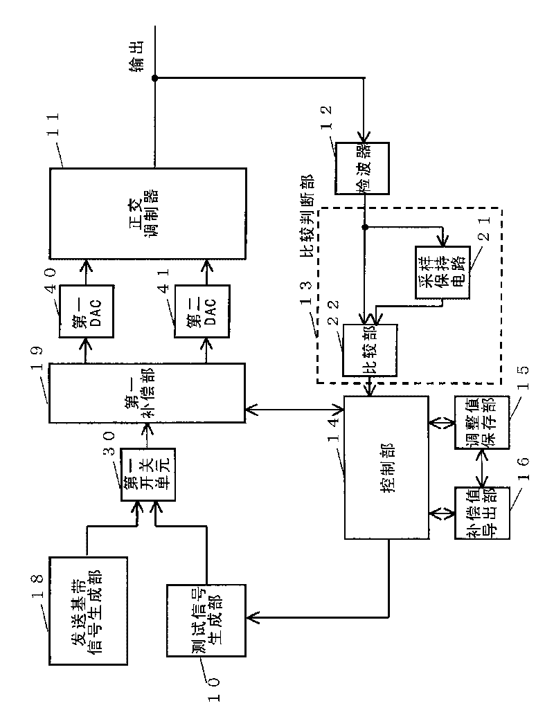
[0119] image 3 It is a figure which shows the signal processing apparatus of 2nd Embodiment of this invention. In addition to this embodiment figure 1 In addition to the structure of the signal processing device, it also includes: a transmission baseband signal generation unit 18 that generates signal components of the I channel and Q channel from the transmission signal, and a unit 17 that estimates the DC offset and the IQ mismatch and inputs the transmission baseband signal. Compensation is performed and the compensated signal is supplied to the first compensation section 19 of the quadrature modulator 11 . The test signal generated by the test signal generating unit 10 is supplied to the quadrature modulator 11 indirectly via the first compensating unit 19 . In addition, it includes: select one of the transmission baseband signal and the test signal and output it to the first switch unit 30 of the first compensating part 19, convert the in-phase component (I) from the ...
no. 3 approach
[0125] Figure 4 is a diagram showing a signal processing device according to a third embodiment of the present invention. In addition to this embodiment figure 1 In addition to the structure of the signal processing device, it also includes: a transmission baseband signal generation unit 18 that generates signal components of the I channel and Q channel from the transmission signal, and a unit 17 that estimates the DC offset and the IQ mismatch and inputs the transmission baseband signal. Compensation is performed and the compensated signal is supplied to the first compensation section 19 of the quadrature modulator 11 . In addition, it includes: the third DAC 42 and the fourth DAC 43 which convert the output of the first compensating part 19 into an analog signal, the fifth DAC 44 and the sixth DAC which convert the test signal generated by the test signal generating part 10 into an analog signal 45. Select one of the output of the third DAC 42 and the output of the fifth...
PUM
 Abstract
Description
Claims
Application Information
 - R&D
- Intellectual Property
- Life Sciences
- Materials
- Tech Scout
- Unparalleled Data Quality
- Higher Quality Content
- 60% Fewer Hallucinations
Browse by: Latest US Patents, China's latest patents, Technical Efficacy Thesaurus, Application Domain, Technology Topic, Popular Technical Reports.
© 2025 PatSnap. All rights reserved.Legal|Privacy policy|Modern Slavery Act Transparency Statement|Sitemap|About US| Contact US: help@patsnap.com