Circuit for improving IO speed

A circuit and speed technology, applied in the field of IO circuits, can solve the problems of long level rise time, long communication time, low data output rate, etc., and achieve the effect of improving communication efficiency, shortening communication time, and improving data transmission speed.

Active Publication Date: 2010-06-23
BEIJING CEC HUADA ELECTRONIC DESIGN CO LTD
View PDF0 Cites 7 Cited by
  • Summary
  • Abstract
  • Description
  • Claims
  • Application Information

AI Technical Summary

Problems solved by technology

Therefore, the IO pins for chip data transmission usually use an open-drain structure PAD, such as figure 1 , when the open-drain PAD outputs low-level to high-level conversion, it is completely completed by the pull-up resistor, and the pull-up resistor is generally tens of K ohms, so that the level rises for a long time and the data output rate is low, the highest is only a few Hundred Kbps baud rate
The communication speed of the ISO7816 serial port is slow and the communication time is too long
On the other hand, with the development of smart card technology, smart cards require higher and higher ETU frequency division ratios, and if the IO speed is too slow, it will also cause functional errors

Method used


Image

  • Circuit for improving IO speed
  • Circuit for improving IO speed
  • Circuit for improving IO speed

Examples


Embodiment Construction

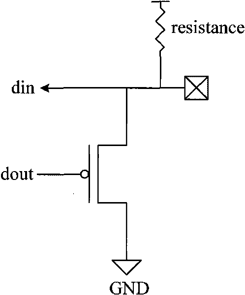
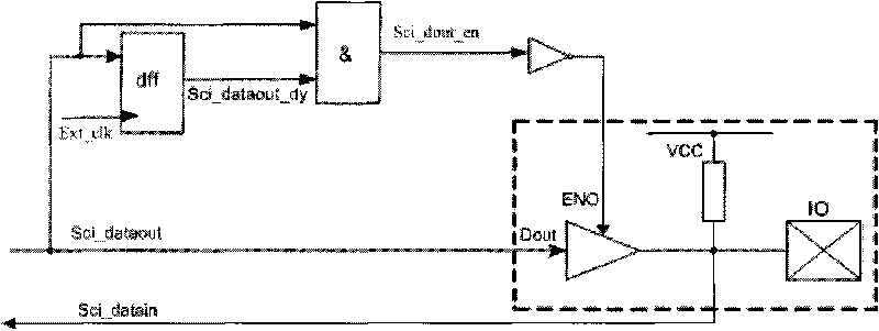
[0011] refer to figure 2 As shown, the open-drain structure proposed by the present invention adds an accelerated conversion pulse of one clock cycle during the "0-1" level conversion, and an IO circuit structure with a pull-up resistor and a tri-state transmission gate structure, including a tri-state bidirectional open-drain IO PAD, a group of logic gate circuits that generate a three-state gate enable signal (ENO).

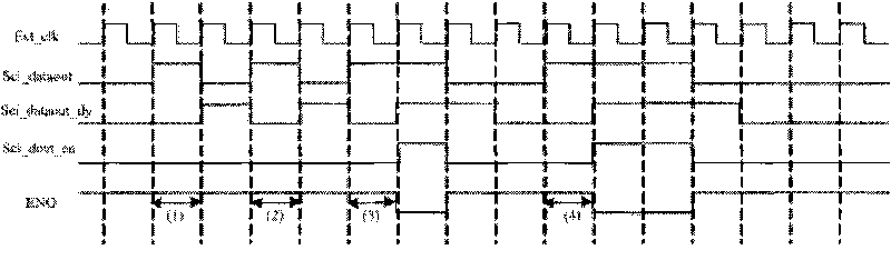
[0012] The serial port output data (Sci_dataout) is locked by a D flip-flop (using the serial port working clock Ext_clk) to generate the Sci_dataout_dy signal. After this signal and the original serial port output data pass through the AND gate, the serial port output data enable signal (Sci_dout_en) is generated. Thus, the serial port data enable signal passes through a NOT gate to generate an enable signal, which is the enable terminal (ENO) signal of the tri-state gate. The three-state gate enable signal ENO generated according to this circuit structure h...


PUM


Abstract

The invention provides a circuit structure for improving the IO speed, i.e. an acceleration conversion pulse is additionally provided with a clock period on an open-drain structure when '0-1' level is converted and an up-pulling resistor and a tristate transmission door are arranged in a structure. The circuit structure comprises tristate bidirectional open-drain IO PAD and a group of logic gate circuits for generating a tristate gate enable signal (EEO). The circuit structure can output a strong drive high level of a period when IO output data generate '0-1' level is converted, also shorten the raising time of the level and effectively improve the communication speed of a 7816 serial port.

Description

technical field [0001] The invention relates to an IO circuit, in particular to a circuit for a contact smart card chip capable of improving the IO communication speed. Background technique [0002] In the field of contact smart cards, the mainstream communication standard is ISO / IEC 7816. The characteristic of this standard is that the bidirectional data transmission pins between the card and the card reader need to be connected in a "wired-AND" manner. Therefore, the IO pins for chip data transmission usually use an open-drain structure PAD, such as figure 1 , when the open-drain PAD outputs low-level to high-level conversion, it is completely completed by the pull-up resistor, and the pull-up resistor is generally tens of K ohms, so that the level rises for a long time and the data output rate is low, the highest is only a few Hundred Kbps baud rate. As a result, the communication speed of the ISO7816 serial port is slow and the communication time is too long. On the o...

Claims


Application Information

Patent Timeline
Patent Type & Authority Applications(China)
IPC IPC(8): G06K19/07
Inventor 周鹏赵贵勇卢锋耿介郑晓光
Owner BEIJING CEC HUADA ELECTRONIC DESIGN CO LTD
Why Eureka
Try Eureka