


Quick Research
Generate reliable direction feasibility study reports for your R&D in just a few steps.

Technical Q&A
Discover and master advanced knowledge NOW. Basics, ideas, possibilities, all at once.

Find Solutions
As an expert in R&D theories, this can generate solutions to your technical problems instantly.

Evaluate Feasibility
Analyze your overall solution with one click, know your potential R&D risks in advance.

Monitor Landscape
Get weekly tech updates, stay abreast of the latest tech innovations and key insights.
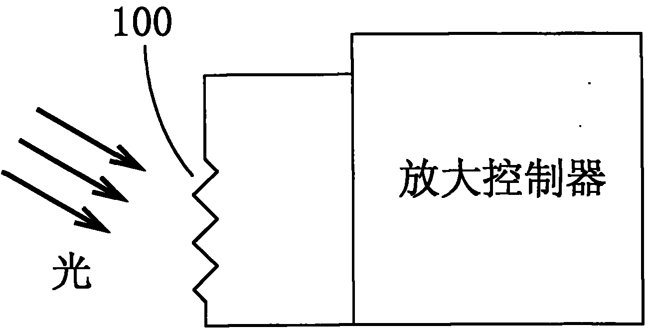
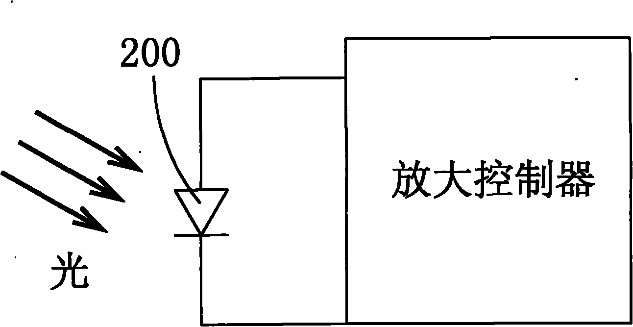
Linear optical sensing device
A sensing device and linear light technology, applied in photometry and circuit measurement using electric radiation detectors, can solve problems such as a single signal cannot sense two-segment signals, and is susceptible to temperature or noise interference
- Summary
- Abstract
- Description
- Claims
- Application Information
AI Technical Summary
Problems solved by technology
Method used
Image

Examples
Embodiment Construction
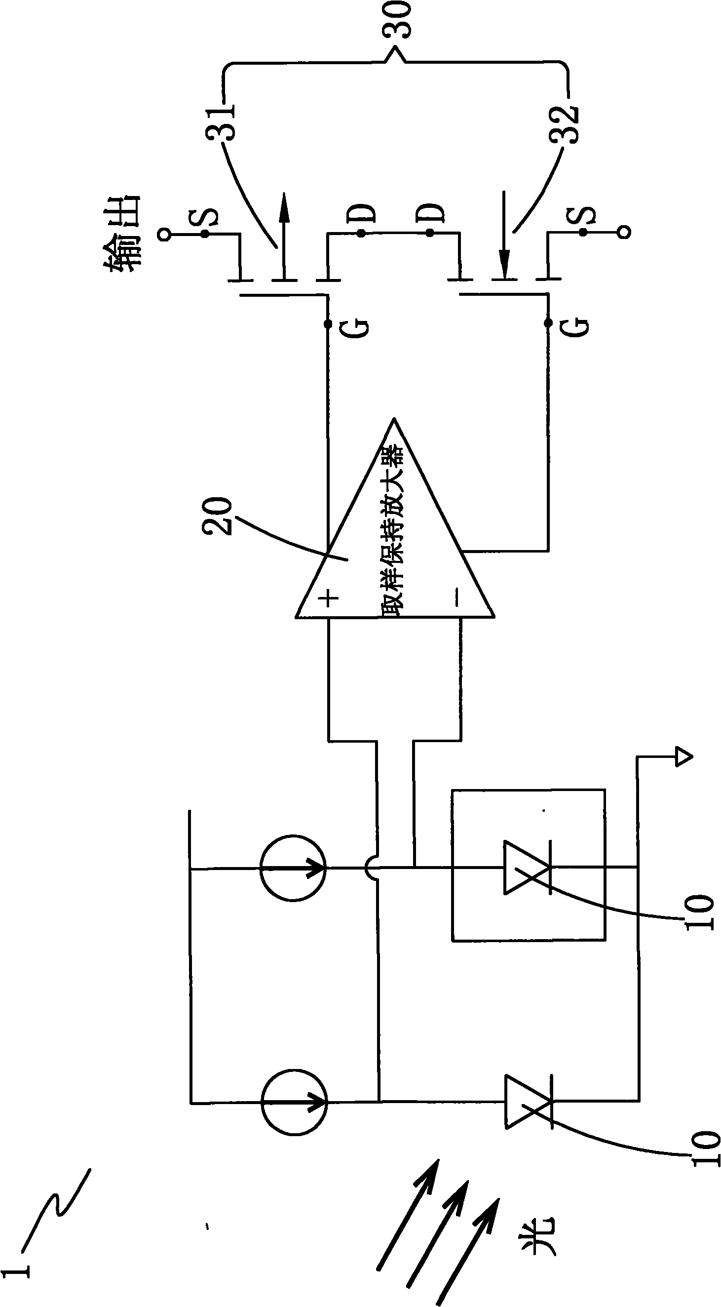
[0013] In order to make it easier for your examiner to understand the content of the present invention and the effects that can be achieved, the detailed descriptions are as follows with reference to the drawings and drawing numbers:
[0014] see image 3 As shown, it is a schematic circuit diagram of the present invention, a linear light sensing device 1, which includes:
[0015] A sampling hold amplifier (sampling hold AMP) 20 is connected with a photosensitive diode 10 at its non-inverting input terminal and its inverting input terminal respectively, and then a group of drivers (Driver) 30 are connected by the output terminal of the sampling hold amplifier 20; , there are two photosensitive diodes 10, the P-type junction of one photosensitive diode 10 is connected to the non-inverting input end of the sample-and-hold amplifier 20, and the P-type junction of the other photosensitive diode 10 is connected to the sample-and-hold amplifier 20 The inverting input terminals of t...
PUM
 Abstract
Description
Claims
Application Information
 - R&D Engineer
- R&D Manager
- IP Professional
- Industry Leading Data Capabilities
- Powerful AI technology
- Patent DNA Extraction
Browse by: Latest US Patents, China's latest patents, Technical Efficacy Thesaurus, Application Domain, Technology Topic, Popular Technical Reports.
© 2024 PatSnap. All rights reserved.Legal|Privacy policy|Modern Slavery Act Transparency Statement|Sitemap|About US| Contact US: help@patsnap.com