Chip debugging method, system and debugging module

A technology for debugging modules and debugging methods, which is applied in digital circuit testing, electronic circuit testing, etc., can solve problems such as chip debugging schemes that cannot work normally and clock matching, and improve debugging efficiency. Die area effect

Inactive Publication Date: 2010-07-07
ISVUE TECH
View PDF0 Cites 10 Cited by
  • Summary
  • Abstract
  • Description
  • Claims
  • Application Information

AI Technical Summary

Problems solved by technology

[0004] The purpose of the present invention is to at least solve one of the above-mentioned technical defects, especially solve the defect that the existing chip debugging scheme cannot match the normal working clock of the system being debugged

Method used


Image

  • Chip debugging method, system and debugging module
  • Chip debugging method, system and debugging module
  • Chip debugging method, system and debugging module

Examples


Embodiment Construction

[0035] Embodiments of the present invention are described in detail below, examples of which are shown in the drawings, wherein the same or similar reference numerals designate the same or similar elements or elements having the same or similar functions throughout. The embodiments described below by referring to the figures are exemplary only for explaining the present invention and should not be construed as limiting the present invention.

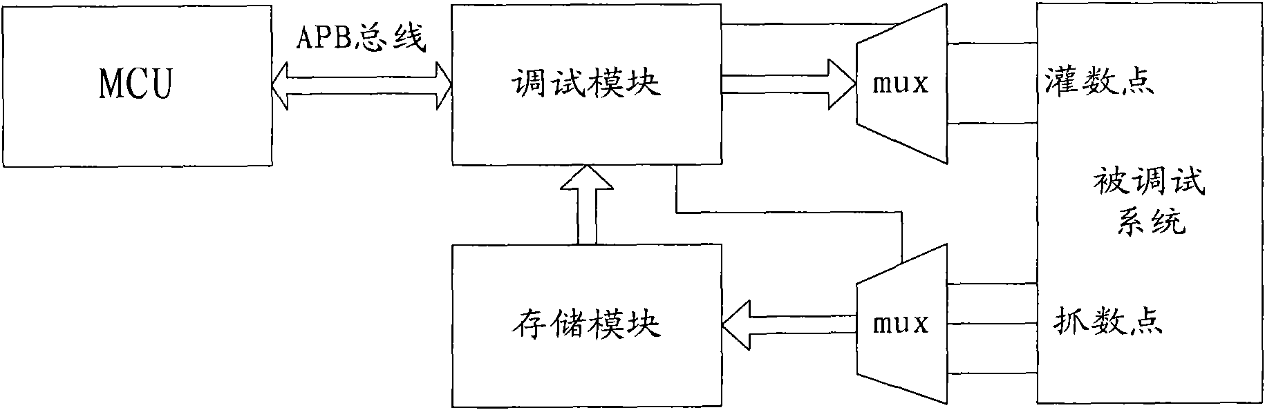
[0036] The present invention mainly lies in that the clock module is controlled by the clock enable signal generated by the debugging module, so that it only turns on the clock of the number point in the system to be debugged when the number is filled, so that the input clock and the system to be debugged are in the normal working clock Matching can not only improve debugging efficiency, but also reduce chip area.

[0037] In addition, as a preferred embodiment of the present invention, when the MCU performs data capture through the debu...


PUM


Abstract

The invention provides a chip debugging method, which comprises the following steps that: a debugging module receives infusion instructions and corresponding infusion points sent by a MCU, and caches infusion data input to the infusion points into a write data register of the debugging module; and when the infusion data cached into the write data register reach a predetermined bit value, the debugging module inputs the cached infusion data to the infusion points, and simultaneously sends a clock enabling signal to a clock module to start the clock of the infusion points during infusing. The MCU realizes the logic control of the debugging module in the chip debugging method by configuring a register of the debugging module through an APB bus, and infusion and capture modes are simple and flexible.

Description

technical field [0001] The invention relates to the technical field of integrated circuit design, in particular to a chip debugging method, system and chip debugging module. Background technique [0002] As the integration and complexity of chips become higher and higher, the debugging in chip design becomes more and more complicated. The purpose of debugging is not only to determine the failure of the chip, but also to find out the cause of the failure. In the debug mode, the designer will pour data into the system to be debugged in a controlled manner, and then read the data from the predetermined data capture point, so as to detect the state of the system to be debugged. However, with the continuous improvement of the chip design level, such as the popularization of technologies such as SOC (System on Chip, System on Chip), the number of irrigation points in the debugged system is also increasing, and the types of irrigation points are also increasing. complex. Because ...

Claims


Application Information

Patent Timeline
Patent Type & Authority Applications(China)
IPC IPC(8): G01R31/317
Inventor 张明明王军阎斌何晶
Owner ISVUE TECH
Why Eureka
Try Eureka