System and method for inspecting a wafer

A detection system and wafer technology, which is applied to TV system parts, measurement devices, optical test flaws/defects, etc., can solve the problem that the semiconductor wafer detection system cannot use bright field and dark field imaging at the same time

Active Publication Date: 2010-07-21
SEMICON TECH & INSTR
View PDF11 Cites 49 Cited by
  • Summary
  • Abstract
  • Description
  • Claims
  • Application Information

AI Technical Summary

Problems solved by technology

However, due to the current lack of technical knowledge and available know-how, memory-based semiconductor wafer inspection systems cannot use both brightfield and darkfield imaging to inspect wafers as they move, while also allowing design and configuration flexibility

Method used


Image

  • System and method for inspecting a wafer
  • System and method for inspecting a wafer
  • System and method for inspecting a wafer

Examples


Embodiment approach 400

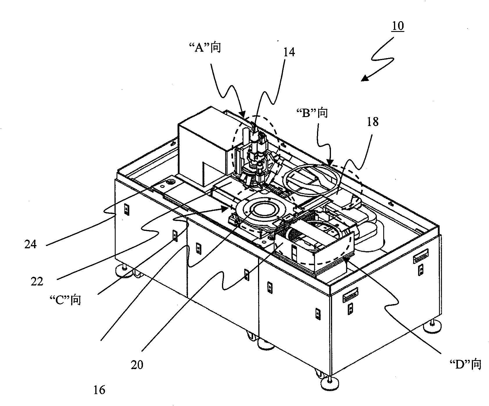
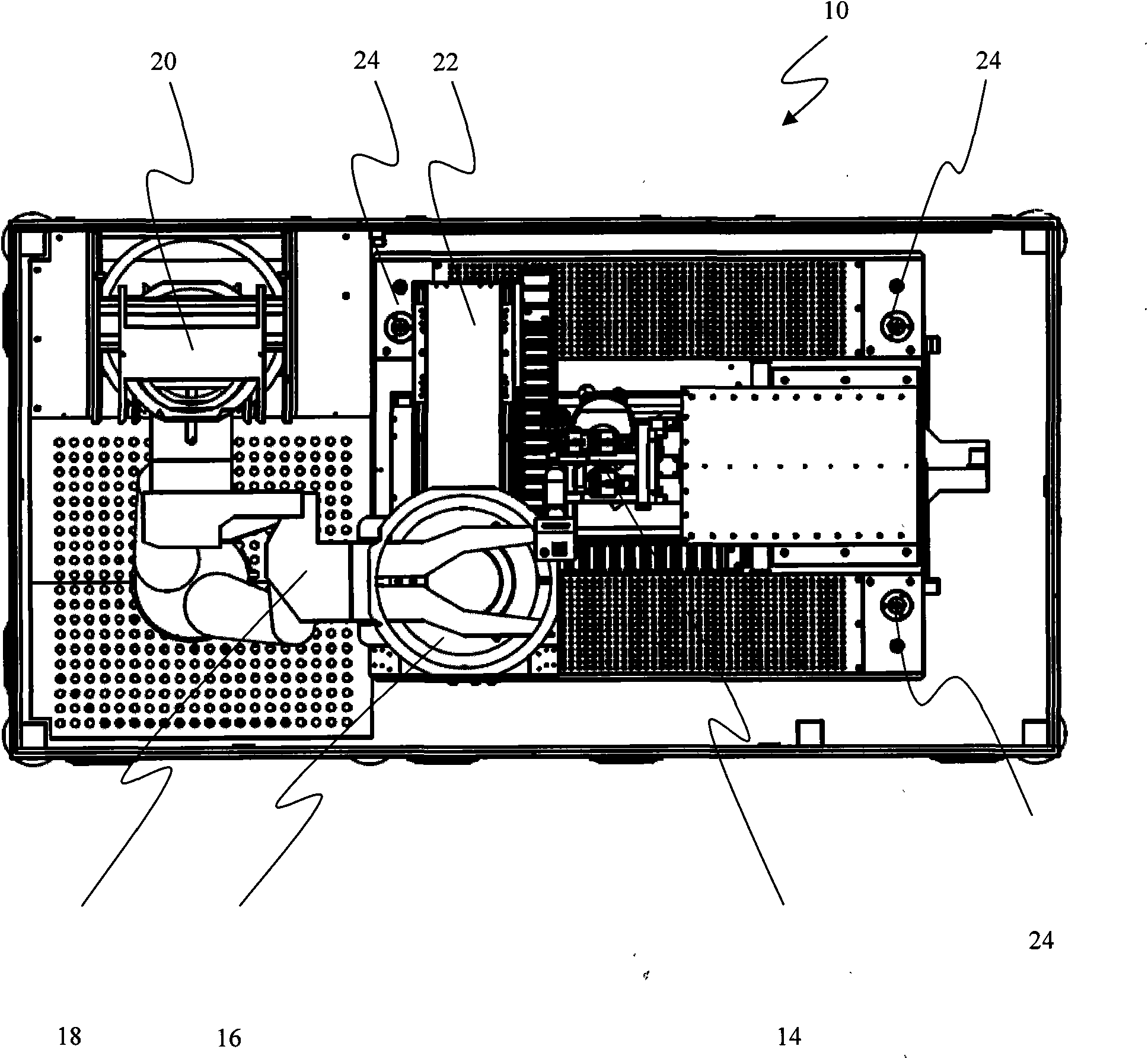
[0181] As mentioned above, the present invention provides an implementation method 400 for inspecting the semiconductor wafer 12, thereby performing at least one of defect detection, classification and review on the semiconductor wafer.

[0182] In step 402 of method 400, semiconductor wafer 12 is loaded onto wafer table 16 by system 10 for inspection, and semiconductor wafer 12 is removed from semiconductor stack 20 and transferred to wafer table 16, preferably by robotic wafer handler 18. . Suction or vacuum is applied to the wafer table 16 to secure the semiconductor wafer on the wafer 12 table.

[0183] Semiconductor wafer 12 preferably contains a wafer identification number or barcode. The above-mentioned wafer identification number or barcode is written or marked on the surface of the semiconductor wafer 12 , specifically at the edge of the surface of the semiconductor wafer 12 . The wafer identification number or barcode is used to identify the semiconductor wafer 12 ...


PUM


Abstract

The present invention provides a method and a system for inspecting a wafer. The system comprises an optical detection head, a wafer operation table, a wafer stack, a XY operation table and a vibration separator. The optical detection head comprises some lighters, an image collector, an objective lens and other optical componets. The system and the method can collect bright field image, dark field image, 3D image and redetection image. The collected image is converted to an image signal and is transmitted to a programmable controller for processing. The detection is performed in the wafer moving process. The collected image is compared with a reference picture for finding the defect on the wafer. The invention provides a process method used for generating an optimized reference image and an optimized process method for detecting the picture. The generation process of the reference picture is performed automatically.

Description

technical field [0001] The invention relates to a wafer detection process. In particular, the invention relates to an automated system and method for inspecting semiconductor components Background technique [0002] Ensuring that semiconductor components, such as semiconductor wafers and chips, are produced at a consistently high quality is increasingly important in the semiconductor industry. Semiconductor wafer fabrication techniques are constantly improving to incorporate an ever increasing number of features on smaller surface areas of semiconductor wafers. Correspondingly, lithographic processes employed in semiconductor wafer fabrication have become more sophisticated to enable the incorporation of increasing numbers of features on smaller surface areas of semiconductor wafers (ie, higher performance of semiconductor wafers). Therefore, the size of latent defects on semiconductor wafers is generally in the micron to sub-micron range. [0003] It is apparent that man...

Claims


Application Information

Patent Timeline
Patent Type & Authority Applications(China)
IPC IPC(8): H01L21/66G01N21/892G01N21/01
CPCG01N21/8806G01N21/9501G06T2207/10152G06T7/001G01N2021/8825G06T2207/30148H01L22/12G06T2207/20212H01L2924/0002H01L2924/00G01B11/30G01N21/88H01L22/00H04N23/74G01N2201/06113G01N2201/0636G06T7/0008
Inventor 阿杰亚拉里·阿曼努拉林靖葛汉成
Owner SEMICON TECH & INSTR
Why Eureka
Try Eureka