Light emitting device

A technology of light-emitting devices and light-emitting elements, which is applied in the direction of light-emitting materials, lighting devices, electroluminescent light sources, etc., and can solve problems such as insufficient color reproducibility of backlights, insufficient color reproducibility of images, and insufficient NTCS ratio.

Active Publication Date: 2010-07-21
NICHIA CORP
View PDF1 Cites 11 Cited by
  • Summary
  • Abstract
  • Description
  • Claims
  • Application Information

AI Technical Summary

Problems solved by technology

When the above-mentioned conventional white light-emitting device is used for the backlight of an image device, the color reproducibility of...

Method used


Image

  • Light emitting device
  • Light emitting device
  • Light emitting device

Examples


Embodiment 1

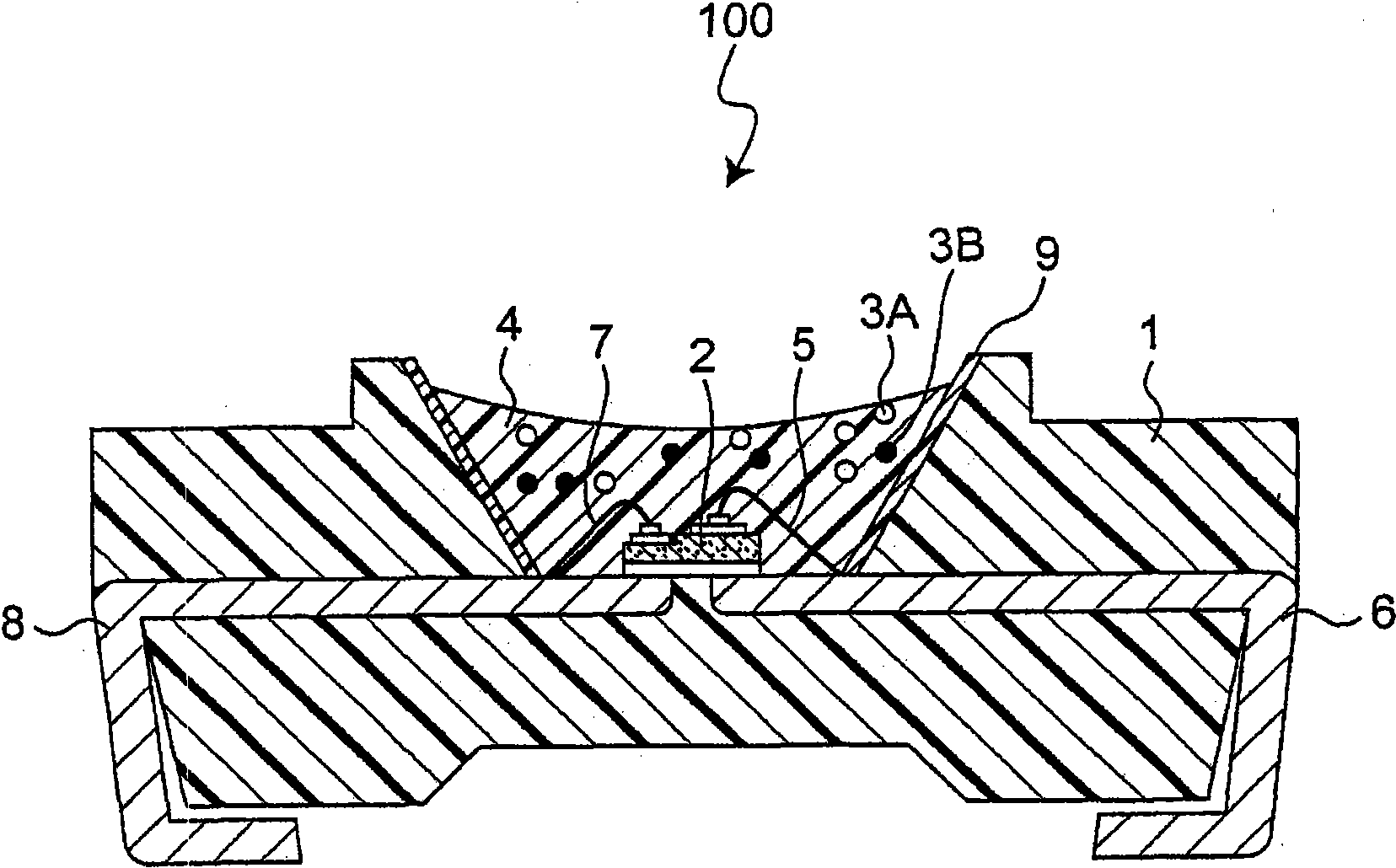
[0155] Melted polyphenolimide resin is poured into the mold in which the positive and negative pair of external electrodes 6 and 8 are inserted and confined, and hardened to form the frame body 1 . The housing 1 has an opening (recess) in which the light emitting element 2 can be accommodated. The frame body 1 and the external electrodes 6 and 8 are integrally molded by cooling the mold.

[0156] On the bottom surface of the concave portion of the frame body 1 formed in this way, a light emitting element (LED chip) 2 having a peak wavelength of 455 nm is chip-mounted with epoxy resin, and then the external electrode 6 and the light emitting element 2 are electrically connected with a conductive bonding wire 5. For connection, the external electrode 8 and the light emitting element 2 are electrically connected with the conductive bonding wire 7 .

[0157] Then, to the silicone resin composition 3 g was added and mixed: a halosilicate Ca having a peak wavelength around 525 nm ...

Embodiment 2

[0164] To the silicone resin composition 3g was added and mixed: halosilicate Ca having a peak wavelength around 520nm 8 MgSi 4 o 16 Cl 2 :Eu((Ca 7.6 , Eu 0.4 )MgSi 4 o 16 Cl 2 ) about 0.3g, and a YAG-based phosphor (Y 2.95 (Al 0.8 , Ga 0.2 ) 5 o 12 : Ce 0.05 )0.1g, and a nitride phosphor CaAlSiBN with a peak wavelength around 660nm 3 :Eu((Ca 0.97 , Eu 0.03 )AlSiBN 3 ) about 0.11g, except that, the light-emitting device 100 was fabricated in the same manner as in Example 1.

[0165] In this embodiment, the difference between the peak wavelength of the green phosphor and the peak wavelength of the YAG-based phosphor is 20 nm, and the addition amount of the YAG-based phosphor is about 20% of the addition amount of all the phosphors.

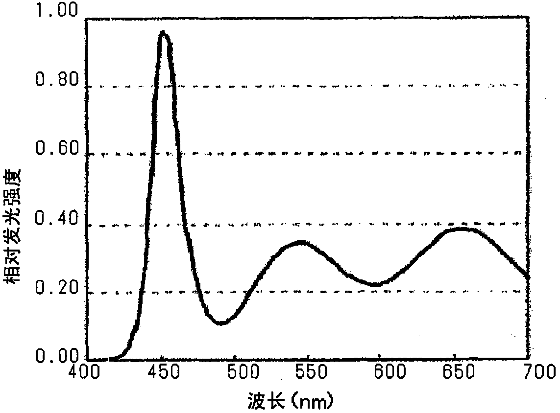
[0166] image 3 is the emission spectrum of the obtained light-emitting device 100 .

[0167] The first peak wavelength is around 450nm, the second peak wavelength is around 520nm, and the third peak wavelength is around 650nm. ...

Embodiment 3

[0171] To the silicone resin composition 3g was added and mixed: halosilicate Ca having a peak wavelength around 520nm 8 MgSi 4 o 16 Cl 2 :Eu((Ca 7.6 , Eu 0.4 )MgSi 4 o 16 Cl 2 ) about 0.3g, and a YAG-based phosphor (Y 2.95 (Al 0.8 , Ga 0.2 ) 5 o 12 : Ce 0.05 )0.15g, and a nitride phosphor CaAlSiBN with a peak wavelength around 660nm 3 :Eu((Ca 0.97 , Eu 0.03 )AlSiBN 3 ) about 0.11g, except that, the light-emitting device 100 was fabricated in the same manner as in Example 1.

[0172] In this example, the difference between the peak wavelength of the green phosphor and the peak wavelength of the YAG-based phosphor was 20 nm, and the added amount of the YAG-based phosphor was about 27% of the added amount of all the phosphors.

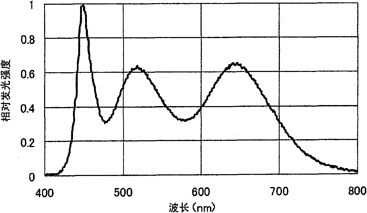
[0173] Figure 4 is the emission spectrum of the obtained light-emitting device 100 .

[0174] The first peak wavelength is around 450nm, the second peak wavelength is around 520nm, and the third peak wavelength is around 640nm.

[01...


PUM


Abstract

Provided is a light emitting device having excellent color reproducing performance. The light emitting device has a light emitting element, a red phosphor composed of a nitride phosphor, and a green phosphor composed of halosilicate. The emission spectrum has a first peak wavelength of 440nm or more but not more than 470nm, a second peak wavelength of 510nm or more but not more than 550nm, and a third peak wavelength of 630nm or more but not more than 670nm. The lowest relative emission strength value between the second peak wavelength and the third peak wavelength is 80% of the lower value of either the relative emission intensity value at the second peak wavelength or the relative emission intensity at the third peak wavelength or is lower than 80% of such value.

Description

technical field [0001] The invention relates to a light emitting device, in particular to a light emitting device containing a light emitting element, a red phosphor and a green phosphor and emitting white light. Background technique [0002] As a light-emitting device having high luminous flux and high color rendering and emitting white light, a light-emitting device having a blue semiconductor light-emitting element and a light emitting element excited by light emitted from the light-emitting element has been proposed. Red phosphors and green phosphors (for example, refer to Patent Document 1). [0003] Among these light-emitting devices, the luminous intensity derived from the red light-emitting component is high, and they are widely used in lighting applications. [0004] Patent Document 1: Japanese Patent Laid-Open No. 2007-2796 [0005] However, white light-emitting devices are used in a variety of applications, and the above-mentioned conventional light-emitting dev...

Claims


Application Information

Patent Timeline
IPC IPC(8): H01L33/00C09K11/08C09K11/59C09K11/64H01L33/50
CPCC09K11/7733C09K11/0883H05B33/14C09K11/774H01L33/504C09K11/7734C09K11/7774H01L2224/48091H01L2224/48465H01L2224/49107H01L2224/73265H01L2924/181H01L2224/32245H01L2224/48247H01L2224/48257C09K11/77342C09K11/77348H01L2924/00014H01L2924/00H01L2924/00012
Inventor 村崎嘉典原田雅史高岛优
Owner NICHIA CORP
Why Eureka
Try Eureka