Method for forming semiconductor device layer by exposure

A technology for semiconductors and devices, applied in the field of exposure to form semiconductor devices as layers, can solve the problems of reduced wafer production efficiency, low work efficiency, large stacking errors, etc., to improve exposure accuracy, production efficiency, and stacking accuracy. The effect of increasing the degree of

Inactive Publication Date: 2010-07-28
SEMICON MFG INT (SHANGHAI) CORP
View PDF0 Cites 7 Cited by
  • Summary
  • Abstract
  • Description
  • Claims
  • Application Information

AI Technical Summary

Problems solved by technology

However, in step 12, the alignment of the exposure table is aligned to the entire wafer of the front layer. However, during the exposure process of the front layer, the exposure unit of the front layer is deformed due to the thermal expansion of the mask plate by the light, resulting in the center , and this deformation cannot be measured in the alignment of the exposure table, so in step 14, use an overlay precision measuring instrument (overlay, OVL) to measure the overlay accuracy of the previous layer and the current layer, The overlay error will be relatively large, and multiple alignment operations need to be performed again, which not only reduces work efficiency, but also reduces wafer production efficiency

Method used


Image

  • Method for forming semiconductor device layer by exposure
  • Method for forming semiconductor device layer by exposure
  • Method for forming semiconductor device layer by exposure

Examples


Embodiment Construction

[0027] In order to make the object, technical solution, and advantages of the present invention clearer, the present invention will be further described in detail below with reference to the accompanying drawings and examples.

[0028] The present invention is described in detail by means of schematic diagrams. When describing the embodiments of the present invention in detail, for the convenience of explanation, the schematic diagrams showing the structure will not be partially enlarged according to the general scale, which should not be used as a limitation of the present invention.

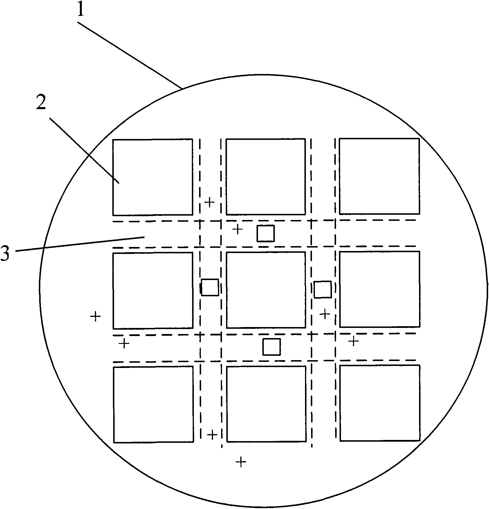
[0029] In the present invention, when the exposure stage is aligned with the front layer, the coordinates of the exposure stage are not only aligned with the coordinates (alignment marks) on the front layer wafer, but also the coordinates of the exposure stage are aligned with the coordinates of the front layer OVL mark. At this time, the characteristic information fed back to the exposure stati...


PUM


Abstract

The invention discloses a method for forming a semiconductor device layer by exposure, which is characterized by comprising that: A, when a lighthouse is aligned with a front layer, the lighthouse measures an alignment mark of the front layer to acquire characteristic information of a front layer wafer, and the lighthouse measures an overlapped precision measuring identifier of the front layer to acquire characteristic information of an exposure unit in the front layer; B, the characteristic information of the front layer wafer and the characteristic information of the exposure unit in the front layer are fed back to the lighthouse; and C, the lighthouse performs exposure to form the layer according to the fed back characteristic information of the wafer and characteristic information of the exposure unit. Due to the adoption of the method, the production efficiency of the wafer can be greatly improved.

Description

technical field [0001] The invention relates to the field of semiconductor manufacturing process, in particular to a method for forming a sublayer of a semiconductor device by exposure. Background technique [0002] Semiconductor devices are fabricated by creating a succession of patterned and unpatterned layers of material in which features on the patterned layer of material are spatially related to each other. Therefore, in the manufacturing process, each patterned material layer must be aligned with the previous patterned material layer, so the overlay accuracy between the previous material layer and the current material layer must be considered. When the semiconductor process develops to provide smaller critical dimensions (Critical Dimensions, CD), reduce the size of the device and increase the complexity of the number of material layers, the quality, reliability and yield of the device, the relationship between the material layer and the material layer Overlay accurac...

Claims


Application Information

Patent Timeline
Patent Type & Authority Applications(China)
IPC IPC(8): G03F7/20G03F9/00
Inventor 肖楠邢一飞
Owner SEMICON MFG INT (SHANGHAI) CORP
Why Eureka
Try Eureka