Self-aligned process for preparing convex graphical substrate

A self-alignment process and graphic substrate technology, which is applied in the direction of electrical components, circuits, semiconductor devices, etc., can solve problems such as instability, polluted cavity etching process, and expensive exposure machine, and achieve the effect of improving uniformity

Active Publication Date: 2010-10-20
EPILIGHT TECH
View PDF4 Cites 7 Cited by
  • Summary
  • Abstract
  • Description
  • Claims
  • Application Information

AI Technical Summary

Problems solved by technology

However, it is very difficult to make a convex pattern substrate now, because it is an isolated small cylindrical pattern microstructure after development. When the pattern height is high, it is difficult to completely retain the pattern during development. Most of the patterns are in the It will be detached during development. In this case, some use a thin metal layer on the upper surface of the substrate, and then do a photolithography process on the upper surface of the metal layer to solve the adhesion of the photoresist. , but some metals will pollute the cavity in the subsequent dry etching process and cause the etching process to be unstable; some use tackifiers, but the effect is not obvious, and it is difficult to mass produce
In addition, especially when the thickness of the photoresist is relatively thick, the precision of the exposure machine cannot be achieved when making convex patterns. If a high-precision stepper exposure machine is used for exposure, it is not achievable by ordinary companies, because such Exposure machines are expensive

Method used


Image

  • Self-aligned process for preparing convex graphical substrate
  • Self-aligned process for preparing convex graphical substrate
  • Self-aligned process for preparing convex graphical substrate

Examples


Embodiment 1

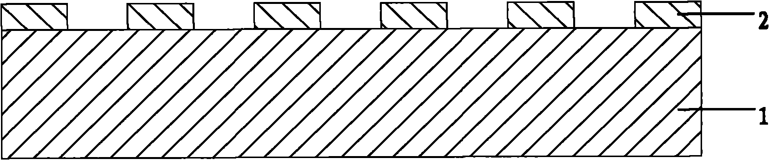
[0029] Step 1, use thinner photoresist on the sapphire substrate to make periodically arranged cylindrical convex pattern microstructures, the height is 0.5um, the maximum width of the cross section is 2um, and the distance between the convex pattern microstructures is 1um.

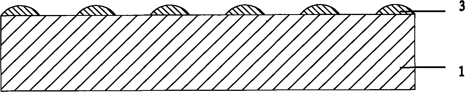
[0030] Step 2, put the sapphire substrate with the convex pattern microstructure into the N 2 High temperature treatment in the atmosphere, the treatment temperature is 450°C, and the treatment time is 10min.

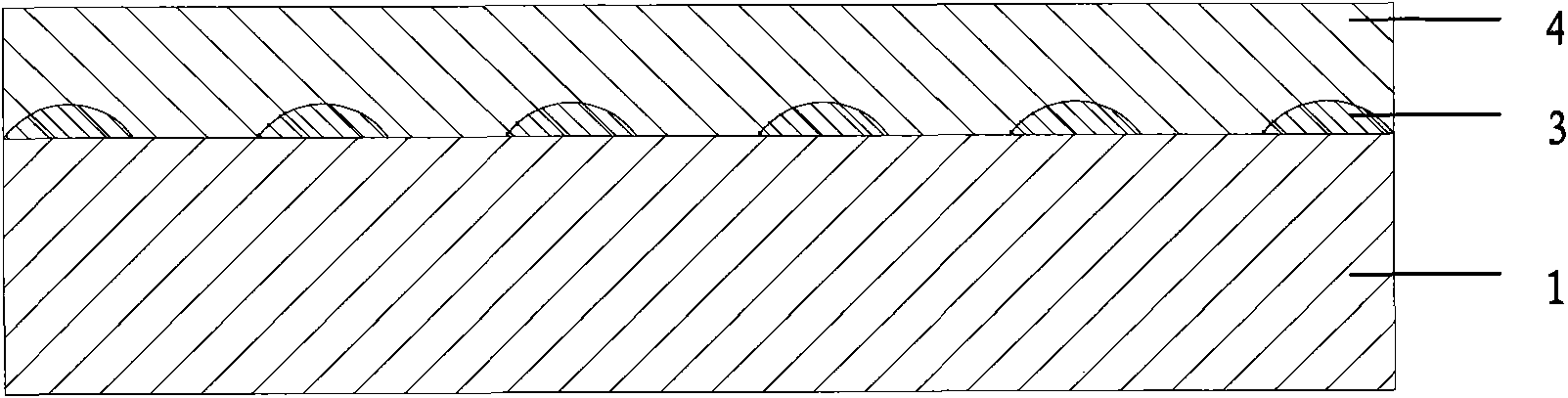
[0031] Step 3: After the high temperature treatment, uniformly coat a photoresist layer with a thickness of 2.5, and perform soft baking.

[0032] Then perform self-alignment exposure, development, high-temperature hardening, and fusion in steps 4-6. Finally, the ICP etching technique is used to transfer the pattern structure of the convex round package to the sapphire substrate to obtain a convex pattern substrate that can be used for nitride epitaxial growth.

Embodiment 2

[0034] Step 1. Use a thinner photoresist to make periodically arranged cylindrical convex pattern microstructures on the sapphire substrate. The height is 0.8um, the maximum width of the cross section is 2.5um, and the distance between each convex pattern microstructure 1.5um.

[0035] Step 2, put the sapphire substrate with the convex pattern microstructure into the N 2 High temperature treatment in the atmosphere, the treatment temperature is 600°C, and the treatment time is 30min.

[0036] Step 3: after the high temperature treatment, uniformly coat a photoresist layer with a thickness of 3.2um, and perform soft baking.

[0037] Then perform self-alignment exposure, development, high-temperature hardening, and fusion in steps 4-6. Finally, the ICP etching technique is used to transfer the pattern structure of the convex round package to the sapphire substrate to obtain a convex pattern substrate that can be used for nitride epitaxial growth.

Embodiment 3

[0039] Step 1: On the sapphire substrate, use a thinner photoresist to make periodically arranged conical convex pattern microstructures, the height is 1um, the maximum width of the cross section is 3um, and the distance between the convex pattern microstructures is 2um .

[0040] Step 2, put the sapphire substrate with the convex pattern microstructure into the N 2 High temperature treatment in the atmosphere, the treatment temperature is 800°C, and the treatment time is 50min.

[0041] Step 3: after the high temperature treatment, uniformly coat a photoresist layer with a thickness of 10 um, and perform soft baking.

[0042] Then perform self-alignment exposure, development, high-temperature hardening, and fusion in steps 4-6. Finally, the ICP etching technique is used to transfer the pattern structure of the convex round package to the sapphire substrate to obtain a convex pattern substrate that can be used for nitride epitaxial growth.


PUM


Abstract

The invention discloses a method for preparing a convex graphical substrate used for the epitaxial growth of nitrides, namely, a self-aligned process for preparing the convex graphical substrate. The method comprises the following steps of: carbonizing a plurality of convex graphical microstructures which are made of thin photoresist and arranged on a sapphire substrate by high-temperature processing; coating a thick photoresist layer on the carbonized microstructures, and carrying out self-aligned exposure on the thick photoresist layer by using the carbonized convex graphical microstructures as a masking film; and fusing the carbonized convex graphical microstructures and the developed photoresist graphs to convex round balls by using high temperature hardening, and finally transferring the graphical structure to the substrate by using the dry etching technology so as to obtain the convex graphical substrate. By adopting the self-aligned process of the invention, the problem that the convex graph made of thick photoresist is easy to drop can be solved, a high-precision exposure requirement can be met by using a common exposure machine, and the uniformity of the graph can be greatly improved, so that the process for preparing the convex graphical substrate can realize industrialization.

Description

technical field [0001] The invention relates to the technical field of semiconductors, in particular to a method for manufacturing a convex pattern substrate for nitride epitaxial growth. Background technique [0002] Light-emitting diodes have the advantages of small size, high efficiency and long life, and are widely used in traffic indication, outdoor full-color display and other fields. In particular, the use of high-power light-emitting diodes may realize semiconductor solid-state lighting, which has caused a revolution in the history of human lighting, and has gradually become a research hotspot in the field of electronics. In order to obtain high-brightness LEDs, the key is to improve the internal quantum efficiency and external quantum efficiency of the device. At present, the light extraction efficiency of the chip is the main factor limiting the external quantum efficiency of the device. The main reason is that the refractive index difference between the epitaxial...

Claims


Application Information

Patent Timeline
Patent Type & Authority Applications(China)
IPC IPC(8): H01L33/20
Inventor 袁根如郝茂盛陈诚
Owner EPILIGHT TECH
Why Eureka
Try Eureka