Glucose detection Cu-based CuO membrane electrode and reparation method thereof
A thin-film electrode and glucose technology, which is used in measuring devices, material analysis by electromagnetic means, instruments, etc., can solve the problems of difficulty in precise control of CuO coating amount, difficulty in uniform dispersion of CuO, and shedding of CuO powder. Linear detection range, short response time, enhanced stability effect
- Summary
- Abstract
- Description
- Claims
- Application Information
AI Technical Summary
Problems solved by technology
Method used
Image
Examples
Embodiment 1
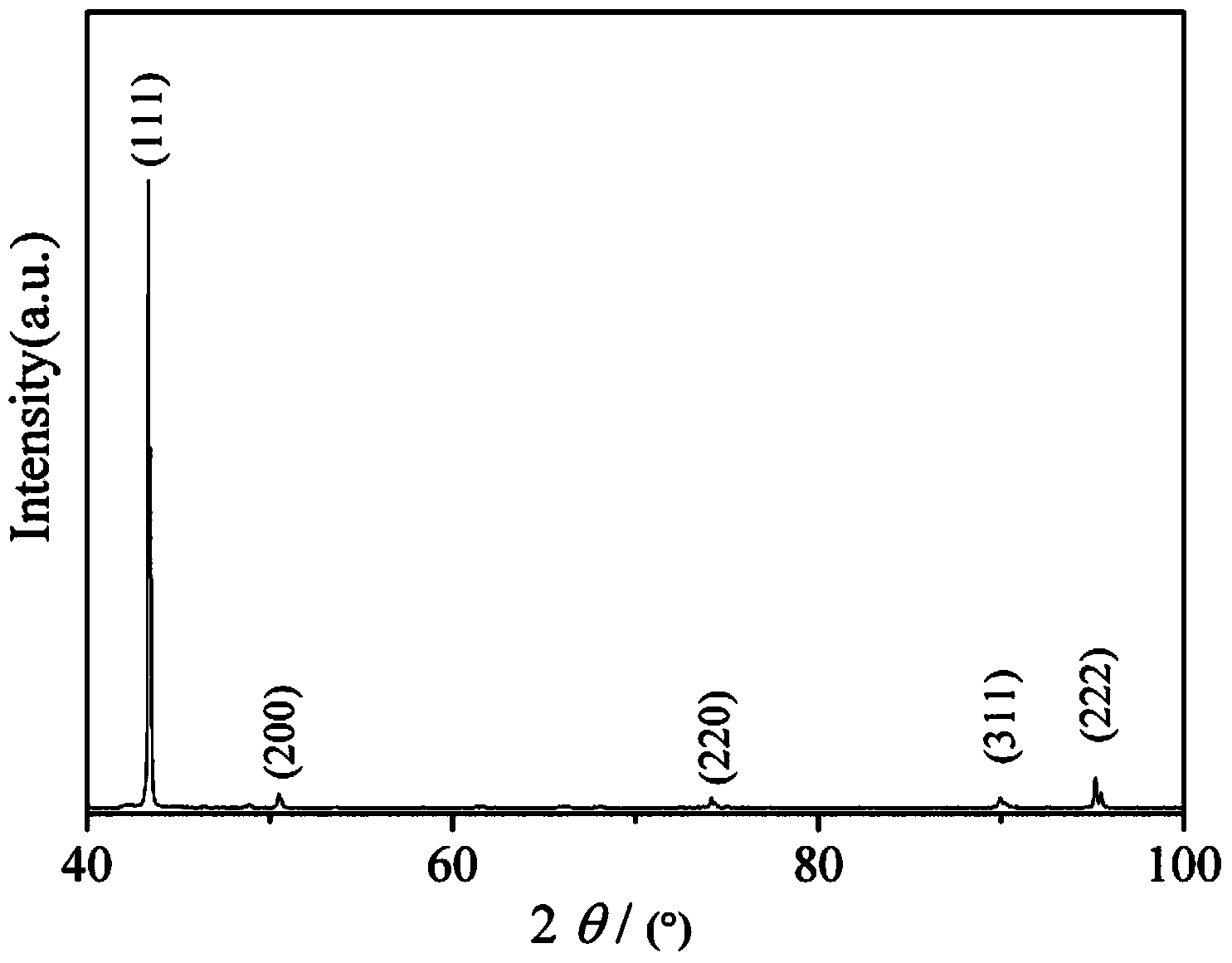
[0027] Step 1. Use a Cu substrate with a highly preferred orientation of (111) crystal plane, ultrasonically degrease the Cu substrate in ethanol, then place it in a 1mol / L HCl solution for ultrasonic etching for 15 minutes, and then use deionized Naturally air-dried after washing with water; the highly preferred orientation of the (111) crystal plane refers to the detection by X-ray diffraction (see X-ray diffraction pattern in figure 2 ), the ratio of the intensity of the diffraction peak of the (111) crystal plane to the intensity of the diffraction peak of the (200) crystal plane is not less than 20; the thickness of the Cu substrate is 1 mm, the length is 50 mm, and the width is 5 mm; the Cu substrate The mass purity is 99.5%;
[0028] Step 2. Place the Cu substrate after natural air-drying in step 1 flatly on the polytetrafluoroethylene platform, and then place it together in a hydrothermal reaction kettle with a tetrafluoroethylene liner with a volume of 500mL. Add 20...
Embodiment 2
[0032] Step 1. Using a Cu substrate with a highly preferred orientation of (111) crystal plane, ultrasonically degrease the Cu substrate in ethanol, then place it in 0.5 mol / L HCl solution for ultrasonic etching for 30 minutes, and then use Naturally air-dried after washing with ionic water; the highly preferred orientation of the (111) crystal plane means that the ratio of the intensity of the diffraction peak of the (111) crystal plane to the intensity of the diffraction peak of the (200) crystal plane is not less than 20 ; The thickness of the Cu substrate is 0.1mm, the length is 20mm, and the width is 10mm; the mass purity of the Cu substrate is 99.9%;
[0033]Step 2. Place the Cu substrate after natural air-drying in step 1 on a polytetrafluoroethylene platform, and then place it together in a hydrothermal reaction kettle with a tetrafluoroethylene liner with a volume of 1000mL. Add 20 mL of deionized water into the gap between the PTFE platforms, and finally seal the hyd...
Embodiment 3
[0037] Step 1. Using a Cu substrate with a highly preferred orientation of (111) crystal plane, ultrasonically degrease the Cu substrate in ethanol, then place it in 0.5 mol / L HCl solution for ultrasonic etching for 30 minutes, and then use Naturally air-dried after washing with ionic water; the highly preferred orientation of the (111) crystal plane means that the ratio of the intensity of the diffraction peak of the (111) crystal plane to the intensity of the diffraction peak of the (200) crystal plane is not less than 20 ; The thickness of the Cu substrate is 1mm, the length is 60mm, and the width is 25mm; the mass purity of the Cu substrate is 99.9%;
[0038] Step 2. Place the Cu substrate after natural air-drying in step 1 on a polytetrafluoroethylene platform, and then place it together in a hydrothermal reaction kettle with a tetrafluoroethylene liner with a volume of 1000mL. Add 40mL of deionized water into the gap between the PTFE platforms, and finally seal the hydro...
PUM
| Property | Measurement | Unit |
|---|---|---|
| thickness | aaaaa | aaaaa |
| width | aaaaa | aaaaa |
| thickness | aaaaa | aaaaa |
Abstract
Description
Claims
Application Information


