Check patentability & draft patents in minutes with Patsnap Eureka AI!

Method for measuring appearance of MEMS (Micro Electro Mechanical System) device based on infrared light interference technique

A topography measurement, infrared light technology, applied in measurement devices, instruments, optical devices, etc., can solve problems such as large measurement errors and difficult operation, and achieve the effects of convenient operation, improved processing technology, and reasonable methods.

Inactive Publication Date: 2010-08-18
ZHONGBEI UNIV
View PDF6 Cites 10 Cited by
  • Summary
  • Abstract
  • Description
  • Claims
  • Application Information

AI Technical Summary

Problems solved by technology

[0005] The present invention provides a MEMS device shape measurement method based on infrared light interference technology in order to solve the problems of difficult operation and large measurement error in measuring the structural shape of MEMS devices with the existing infrared light interference technology

Method used


Image

  • Method for measuring appearance of MEMS (Micro Electro Mechanical System) device based on infrared light interference technique
  • Method for measuring appearance of MEMS (Micro Electro Mechanical System) device based on infrared light interference technique
  • Method for measuring appearance of MEMS (Micro Electro Mechanical System) device based on infrared light interference technique

Examples


Embodiment Construction

[0039] The MEMS device shape measurement method based on infrared light interference technology is realized in the following steps:

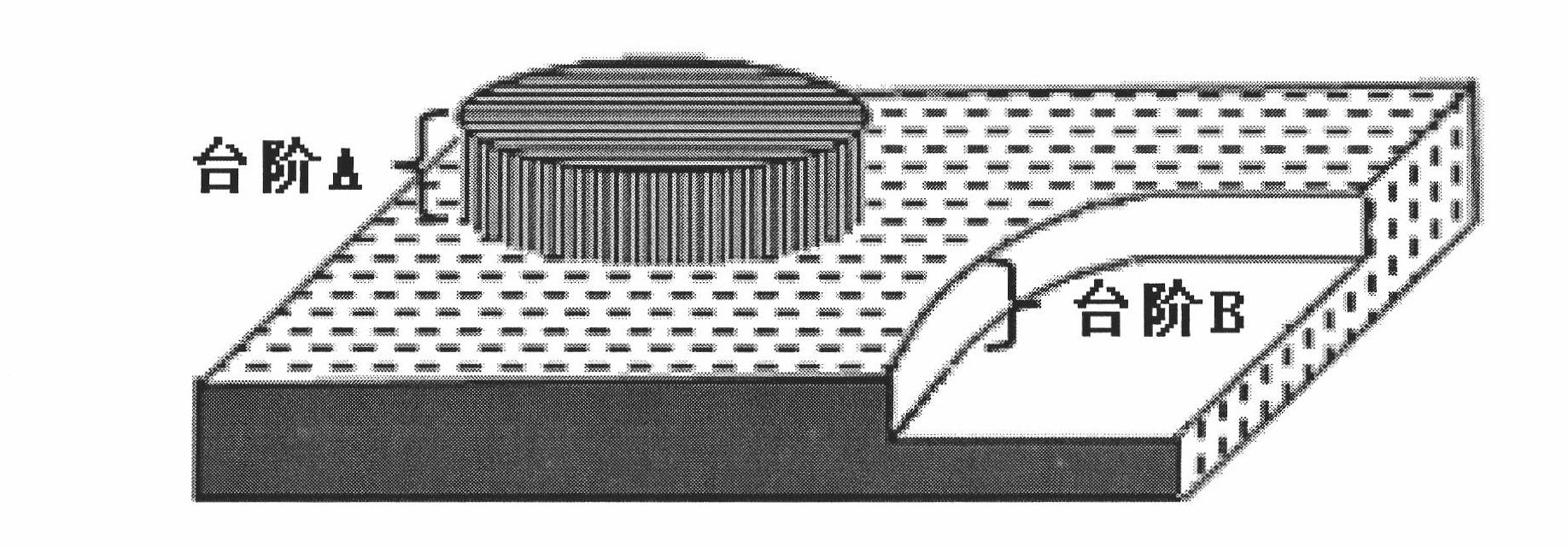
[0040] 1), MEMS device 7 to be tested is prepared before measurement: on the basis of not damaging the topography of the surface to be measured of MEMS device 7 to be measured, non-destructive treatment is carried out on the surface to be measured of MEMS device 7 to be measured to prevent infrared transmission (such as the content of the invention In the verification test, the gold layer 12) that is plated on the surface of the MEMS device to be tested; and after processing, it is placed on the interferometer scanning platform, and the surface to be measured of the MEMS device 7 to be tested is scanned downward toward the interferometer platform;

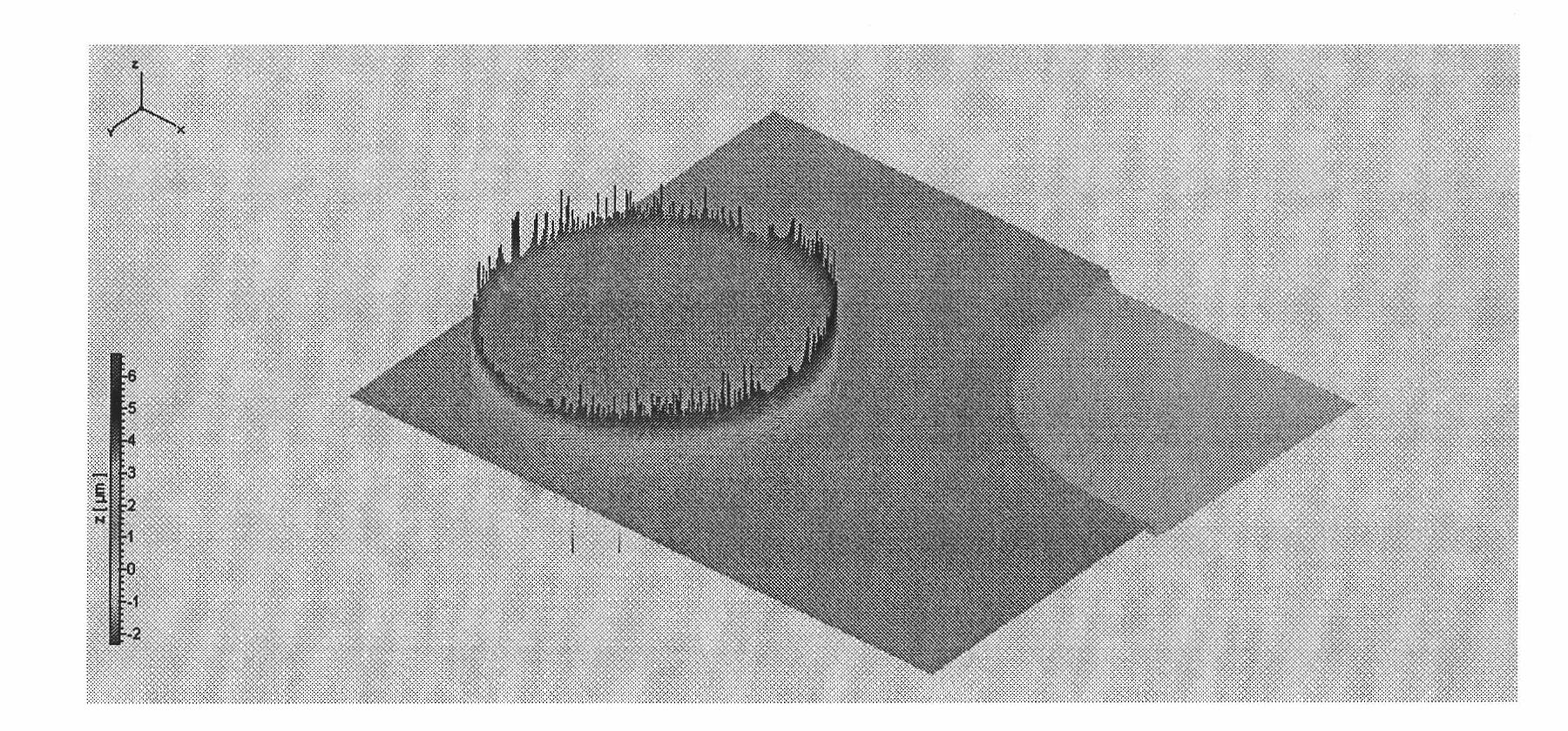
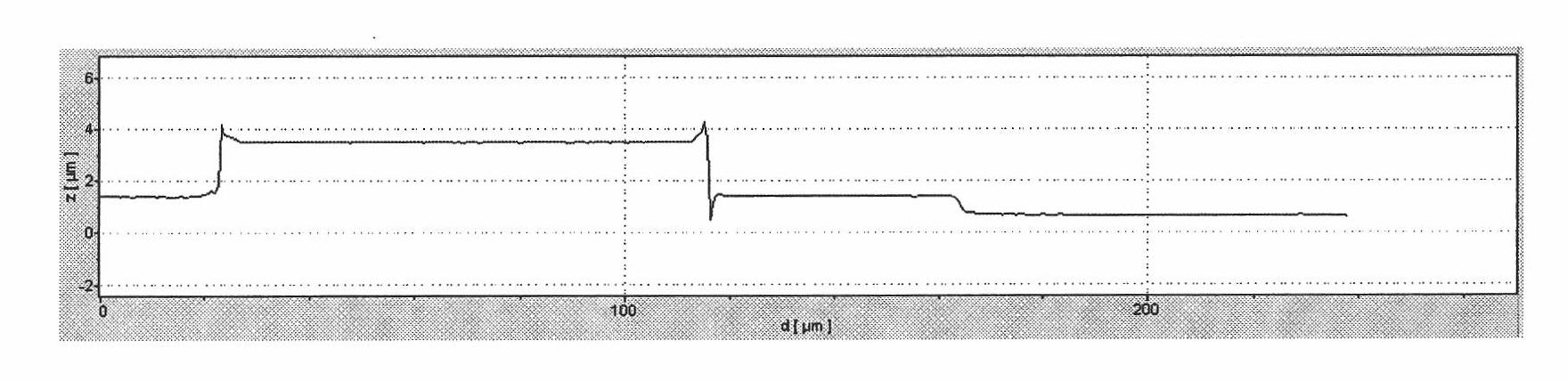
[0041] 2) Use an interferometer to measure the MEMS device to be tested: such as Figure 4 as shown,

[0042] a. Taking the infrared light source 1 as the measurement light source, the infrared lig...


PUM

PropertyMeasurementUnit
Center wavelengthaaaaaaaaaa
Half widthaaaaaaaaaa

Abstract

The invention relates to appearance testing of an MEMS (Micro Electro Mechanical System) device, in particular to a method for measuring the appearance of an MEMS device based on an infrared light interference technique, which solves the problems of difficult operation, larger measurement error and the like when the structure appearance of the MEMS device is measured by the traditional infrared light interference technique. The method for measuring the appearance of the MEMS device based on the infrared light interference technique comprises the following steps of: (1) preparing the MEMS device to be measured before measurement; (2) measuring the MEMS device to be measured by using an interferometer, and arranging a semiconductor wafer, the material quality of which is the same as the material quality of the MEMS device to be measured in front of an optical lens of a reference path. The method is reasonable and convenient in operation, can accurately embody the appearance condition of the microstructure of the MEMS device, is beneficial to quality evaluation of the MEMS device, provides a basis for improving the machining technology and the machining processes of the MEMS device, promotes the improvement of the quality and the using performance of the MEMS device, and is suitable for the fields of reconstruction of the internal structure of the MEMS device based on semiconductor materials, evaluation of the roughness of the bonding interface of a bonding sample, real-time and on-line detection of the MEMS technology, and the like.

Description

technical field [0001] The invention relates to the appearance test of MEMS devices, in particular to a method for measuring the appearance of MEMS devices based on infrared light interference technology. Background technique [0002] With the development of MEMS, the requirements for MEMS devices are getting higher and higher. Among them, the surface morphology of MEMS devices is an important index in the quality evaluation of devices, which directly affects the quality and performance of devices. . [0003] At present, great progress has been made in the application of white light interferometry to measure the surface topography of MEMS devices at home and abroad. Among them, the principle of white light interferometry measurement is: the light source is divided into two beams by a beam splitter at a 45-degree angle, one beam is used as a reference beam, and the other beam is used as a measurement beam. The measurement beam is reflected by the measured object and interfer...

Claims


Application Information

Patent Timeline
IPC IPC(8): G01B11/24
Inventor 薛晨阳丑修建张文栋熊继军刘俊牛康康刘毅刘君
Owner ZHONGBEI UNIV
Features
  • R&D
  • Intellectual Property
  • Life Sciences
  • Materials
  • Tech Scout
  • Unparalleled Data Quality
  • Higher Quality Content
  • 60% Fewer Hallucinations
Learn More