Eureka AIR delivers breakthrough ideas for toughest innovation challenges, trusted by R&D personnel around the world.

Multispectral photosensitive component

A photosensitive device, multi-spectral technology, applied in the direction of electric solid-state devices, semiconductor devices, semiconductor/solid-state device manufacturing, etc. Practical value and other issues, to achieve the effect of good color sensitivity, good flexibility, and improved sensitivity

Active Publication Date: 2010-08-18
BOLY MEDIA COMM SHENZHEN
View PDF4 Cites 20 Cited by
  • Summary
  • Abstract
  • Description
  • Claims
  • Application Information

AI Technical Summary

Problems solved by technology

Although Foveon's X3 three-layer photosensitive technology uses depth to achieve color selection, eliminating the need for filter films, but the production of three-layer photosensitive technology is already very difficult and the industrialization situation is not good. If an infrared layer is added below, then , the situation will only become more complicated, so it is difficult to have practical value
The second reason is that silicon, which is commonly used in semiconductors, usually only absorbs infrared light at wavelengths below 1100 nanometers.
These materials are not suitable for use in visible light
The third is the lack of practical double-layer or multi-layer photosensitive device manufacturing technology

Method used


Image

  • Multispectral photosensitive component
  • Multispectral photosensitive component
  • Multispectral photosensitive component

Examples


Embodiment Construction

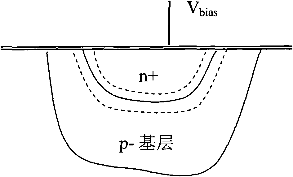
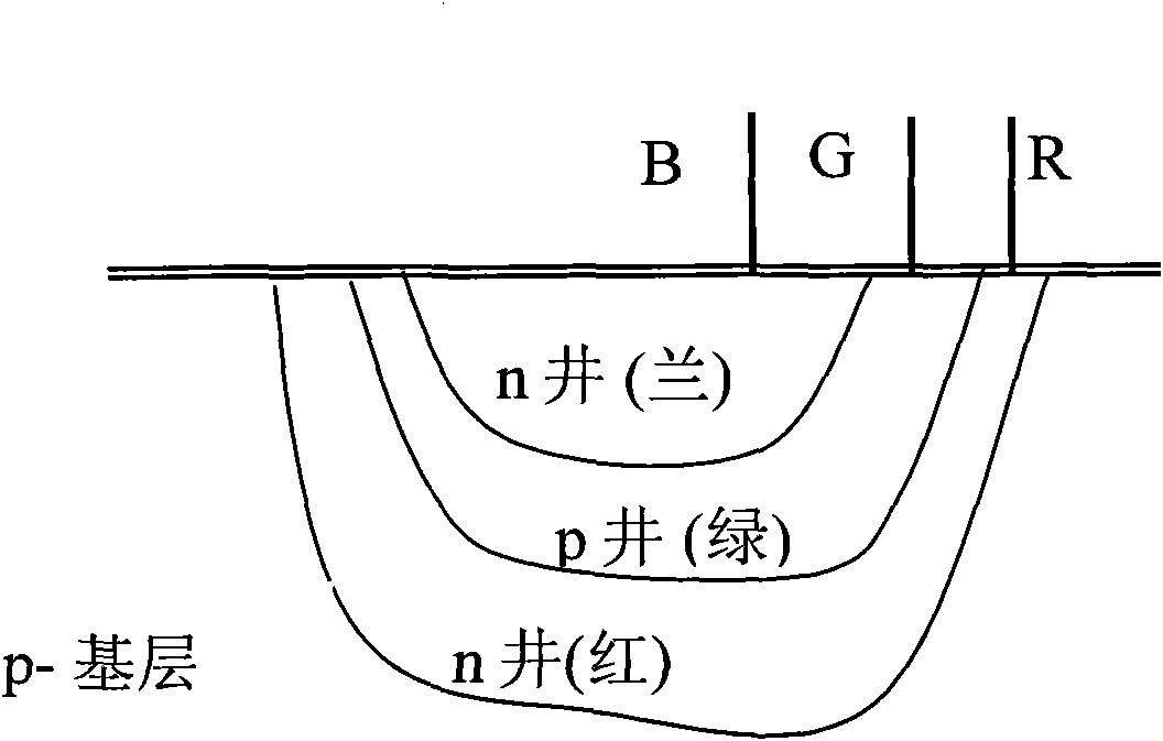
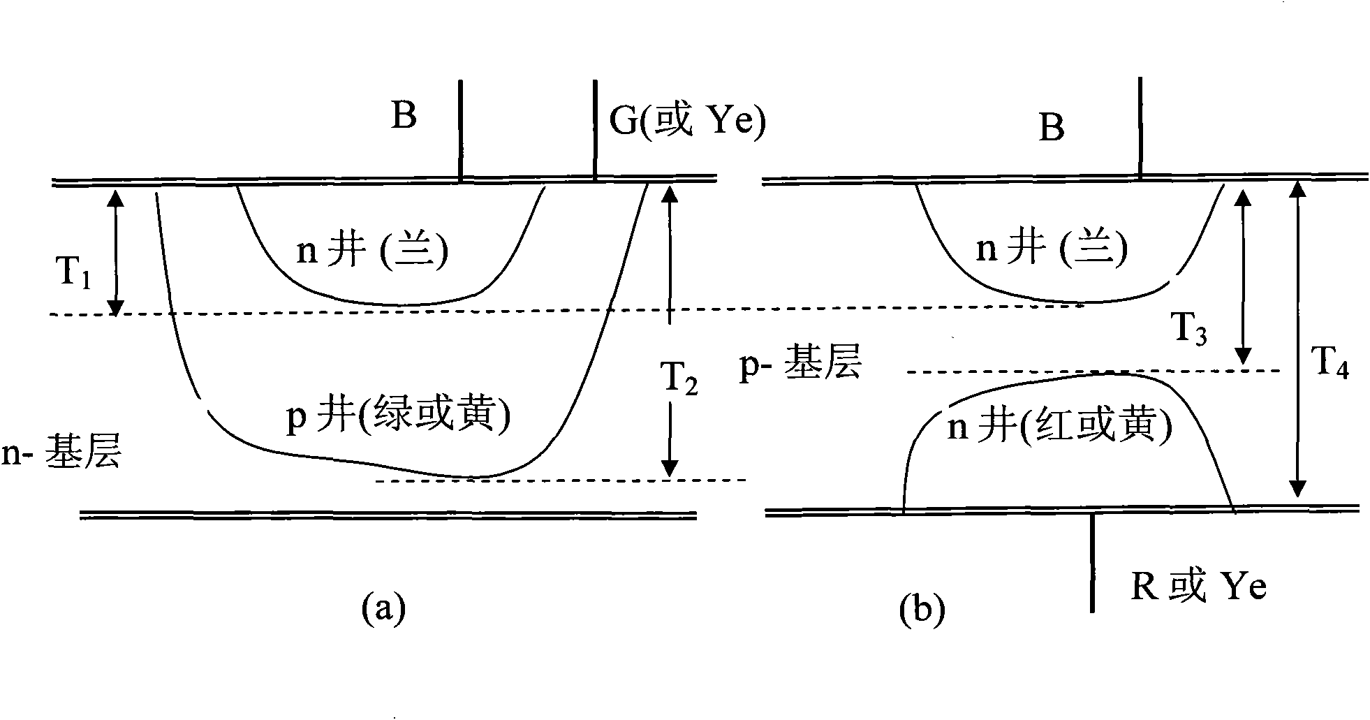
[0065] For the convenience of describing the present invention and explaining the difference between it and the prior art, we now give definitions of the following terms: double-layer photosensitive device, multilayer photosensitive device, double-sided photosensitive device, and bidirectional photosensitive device. Among them, the double-layer photosensitive device means that the photosensitive pixels are physically divided into two layers, and each layer contains photosensitive pixels that sense a specific spectrum. A multi-layer photosensitive device refers to a photosensitive device with more than two layers, such as the X3 photosensitive device of Foveon Company. A double-sided photosensitive device means that the photosensitive device has two photosensitive surfaces, each of which can receive light from at least one direction. A bidirectional photosensitive device means that the photosensitive device can receive light from two directions (usually 180 degrees to each othe...


PUM


Abstract

The invention relates to a multispectral photosensitive component which comprises multilayer composite photosensitive pixels which adopt a single-face or double-face machining mode, realize up-down placement in a silicic P or N basic layer in two, three or four and respectively induct spectra which are orthogonal or complementary in visible light or visible and infrared light spectra. Basic photosensitive pixels on different levels in the composite photosensitive pixels can be designed to induct different colors or spectra, therefore, a multispectral photosensitive chip is obtained by repeatedly arranging a macro unit comprising more than one composite photosensitive pixel. The multispectral photosensitive component comprises a new design of the multilayer photosensitive pixels and examples thereof used for single-face double-layer, double-face double-layer, double-face three-layer, double-face four-layer, single-face mixed double-layer and double-face mixed double-layer or multilayermultispectral photosensitive components. The multispectral photosensitive component has more favorable colored photosensitive property and colored photosensitive and infrared photosensitive integration and simple machining process.

Description

technical field [0001] The invention relates to a multi-spectrum photosensitive device, in particular to the physical realization and manufacture of a multi-spectral photosensitive device. More precisely, the present invention relates to a photosensitive device for full-color images that can simultaneously sense multiple spectra (such as visible light and infrared rays) using CCD or CMOS semiconductors. Here, panchromatic refers to the entire spectrum of interest. For ordinary (visible light) photosensitive devices, panchromatic refers to covering the entire visible spectrum of red, green, blue and white. For photosensitive devices that combine infrared and color, panchromatic refers to the visible spectrum and the infrared spectrum. The invention is applicable to multi-spectral photosensitive devices including infrared, black and white and color images. Background technique [0002] The present invention is a continuation of "Multi-spectral photosensitive device and its ...

Claims


Application Information

Patent Timeline
IPC IPC(8): H01L27/14H01L21/20
CPCH01L27/14647H01L27/14612H01L27/14641H01L27/14652
Inventor 胡笑平
Owner BOLY MEDIA COMM SHENZHEN
Why Eureka
Eureka Blog
Learn More