Nand memory cell array, nand flash memory having nand memory cell array, data processing method for nand flash memory

A technology of memory array and processing method, which is applied in the data processing field of NAND gate memory array grid and NAND flash memory, and can solve difficult reverse and gate structure programming method, interference, gate voltage increase Large and other problems, to achieve the effect of size reduction, low power operation, and lower operating voltage

Inactive Publication Date: 2010-08-18
崔雄林
View PDF0 Cites 1 Cited by
  • Summary
  • Abstract
  • Description
  • Claims
  • Application Information

AI Technical Summary

Problems solved by technology

However, since the change in the charge storage state of the transfer transistor causes a disturbance phenomenon, there is a limit to the increase of the gate voltage
For this reason, hot carrier injection schemes that require passing high currents and high voltages across multiple series-connected storage transistors are difficult to use in programming methods for traditional NAND gate structures.

Method used


Image

  • Nand memory cell array, nand flash memory having nand memory cell array, data processing method for nand flash memory
  • Nand memory cell array, nand flash memory having nand memory cell array, data processing method for nand flash memory
  • Nand memory cell array, nand flash memory having nand memory cell array, data processing method for nand flash memory

Examples


Embodiment Construction

[0049] Hereinafter, exemplary embodiments of the present invention will be described in more detail with reference to the accompanying drawings.

[0050] First, the main idea of ​​the present invention is described.

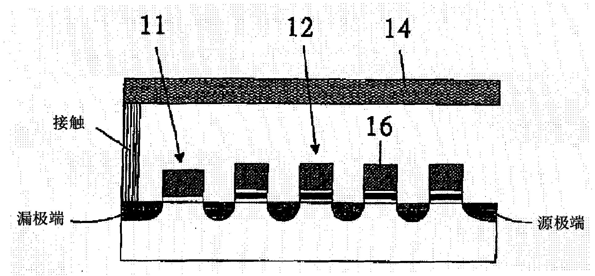
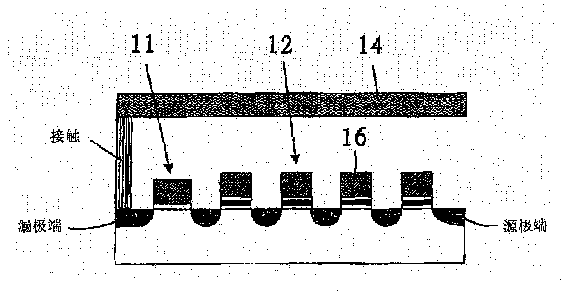
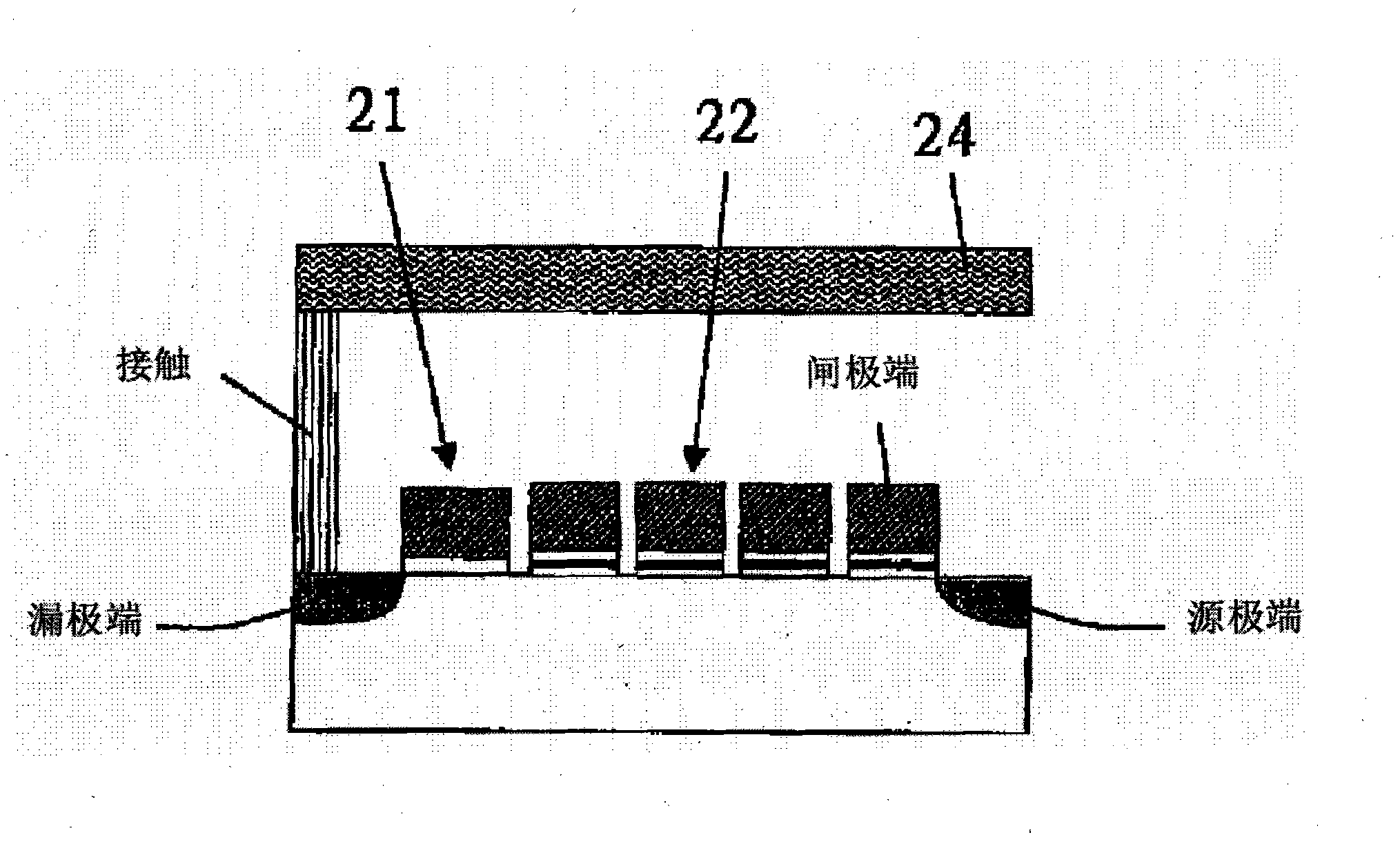
[0051] In the NAND flash memory according to the present invention, a drain terminal selection transistor is disposed between the bit line and one terminal of one of the storage transistors connected in series, and a source line is directly connected to the other terminal of the storage transistor. a terminal. Therefore, the hot carrier injection scheme can be used to realize NAND flash memory with only one select transistor under the following bias conditions.

[0052] In conventional NAND flash memory, since the FN tunneling scheme is used for writing data, an NAND flash memory structure has been proposed which has a drain select transistor connected to the bit line and a source select transistor connected to the source line. However, according to the presen...


PUM


Abstract

A NAND memory cell array which can be programmed in a hot carrier injection scheme, a NAND flash memory having the NAND memory cell array, and a data processing method for the NAND flash memory are provided. The NAND memory cell array includes one select transistor and at least two storage transistors. The NAND memory cell array can be programmed by controlling a bulk bias voltage and a voltage applied to a gate in the hot carrier injection scheme.

Description

technical field [0001] The present invention relates to a kind of flash memory, more specifically, relate to a kind of NAND memory array grid that can be programmed in low current, low voltage, and low power consumption, have the NAND gate memory array grid An NAND flash memory and a data processing method for the NAND flash memory. Background technique [0002] According to the array scheme of the memory cell arranged between the bit line and the ground line, the flash memory structure can be mainly divided into an NOR flash memory structure and an NAND gate flash memory structure. In NOR flash memory, memory cells are arranged in parallel between the bit line and the ground line. In NAND flash memory, cells are arranged in series between a bit line and a ground line. [0003] In NOR flash memory, a hot carrier injection scheme is used to program memory cells, that is, store data in the memory cells, and a Fowler-Nordheim (FN) tunneling scheme is used to erase memory cell...

Claims


Application Information

Patent Timeline
Patent Type & Authority Applications(China)
IPC IPC(8): G11C16/02
CPCG11C16/3418G11C16/0483G11C16/10G11C5/02H10B41/35
Inventor 崔雄林
Owner 崔雄林
Why Eureka
Try Eureka