Homeotropic alignment type pixel structure and manufacturing method thereof
A technology of pixel structure and vertical alignment, which is applied in semiconductor/solid-state device manufacturing, optics, instruments, etc., and can solve the problems of pixel electrical influence, light leakage current of thin film transistors, and thickness increase.
- Summary
- Abstract
- Description
- Claims
- Application Information
AI Technical Summary
Problems solved by technology
Method used
Image


Examples
Embodiment Construction
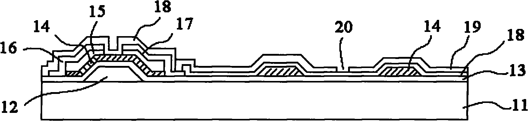
[0040] Please refer to Figure 2A --2E, Figure 2A -- 2E is a schematic diagram of the process steps of the vertical alignment pixel structure of the present invention.
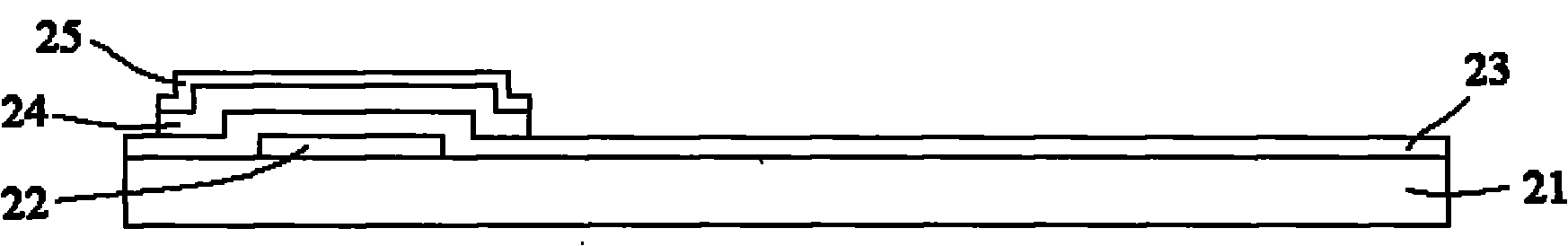
[0041] Such as Figure 2A As shown, first, a substrate 21 is provided, and a first metal layer is formed on the substrate 21 , and then, the first metal layer is patterned to form a gate 22 .
[0042] Please refer to Figure 2B ,exist Figure 2A On the basis of this, a gate insulating layer 23 is formed on the substrate 21 and covers the gate 22 . Then, an amorphous silicon layer is formed on the gate insulating layer 23 , and a doped amorphous silicon layer is formed on the amorphous silicon layer. Next, pattern the amorphous silicon layer and the doped amorphous silicon layer to form the gate amorphous silicon region 24 and the doped gate amorphous silicon region 25, and the gate amorphous silicon region 24 and the doped gate amorphous silicon region The crystalline silicon region 25 is correspondingl...
PUM
 Abstract
Description
Claims
Application Information
 - R&D
- Intellectual Property
- Life Sciences
- Materials
- Tech Scout
- Unparalleled Data Quality
- Higher Quality Content
- 60% Fewer Hallucinations
Browse by: Latest US Patents, China's latest patents, Technical Efficacy Thesaurus, Application Domain, Technology Topic, Popular Technical Reports.
© 2025 PatSnap. All rights reserved.Legal|Privacy policy|Modern Slavery Act Transparency Statement|Sitemap|About US| Contact US: help@patsnap.com