Manufacturing method of polycrystalline silicon film material

A technology of polysilicon thin film and manufacturing method, which is applied in semiconductor/solid-state device manufacturing, electrical components, circuits, etc., can solve the problems of induced metal residue, uncontrollable induced metal diffusion, and long crystallization time, so as to improve grain size, Effect of reducing metal residue and shortening time

Inactive Publication Date: 2010-09-15
GUANGDONG SINODISPLAY TECH
View PDF0 Cites 5 Cited by
  • Summary
  • Abstract
  • Description
  • Claims
  • Application Information

AI Technical Summary

Problems solved by technology

[0004] Among the known metal-induced crystallization film manufacturing technologies, the lateral metal-induced crystallization film technology obtains the best material and device performance, while the metal-induced crystallization film In order for the manufacturing technology to be practical, the following problems need to be solved urgently: 1. High concentration of induced metal residues; 2. Unable to control the diffusion of induced metals; 3. Long crystallization time

Method used


Image

  • Manufacturing method of polycrystalline silicon film material
  • Manufacturing method of polycrystalline silicon film material
  • Manufacturing method of polycrystalline silicon film material

Examples


example 6

[0060] According to an example of the present invention (taking Example 6 as an example), the method for preparing polysilicon thin film material comprises the following steps:

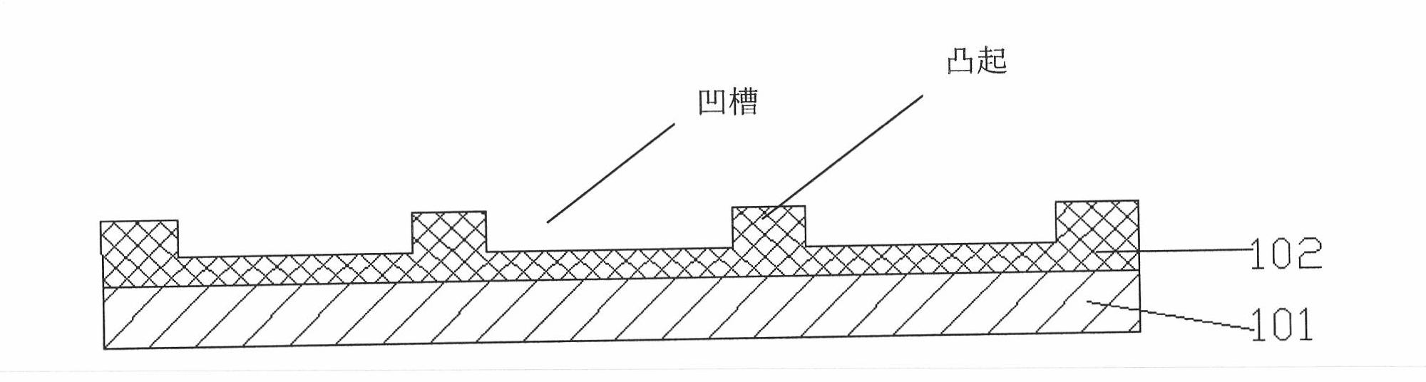
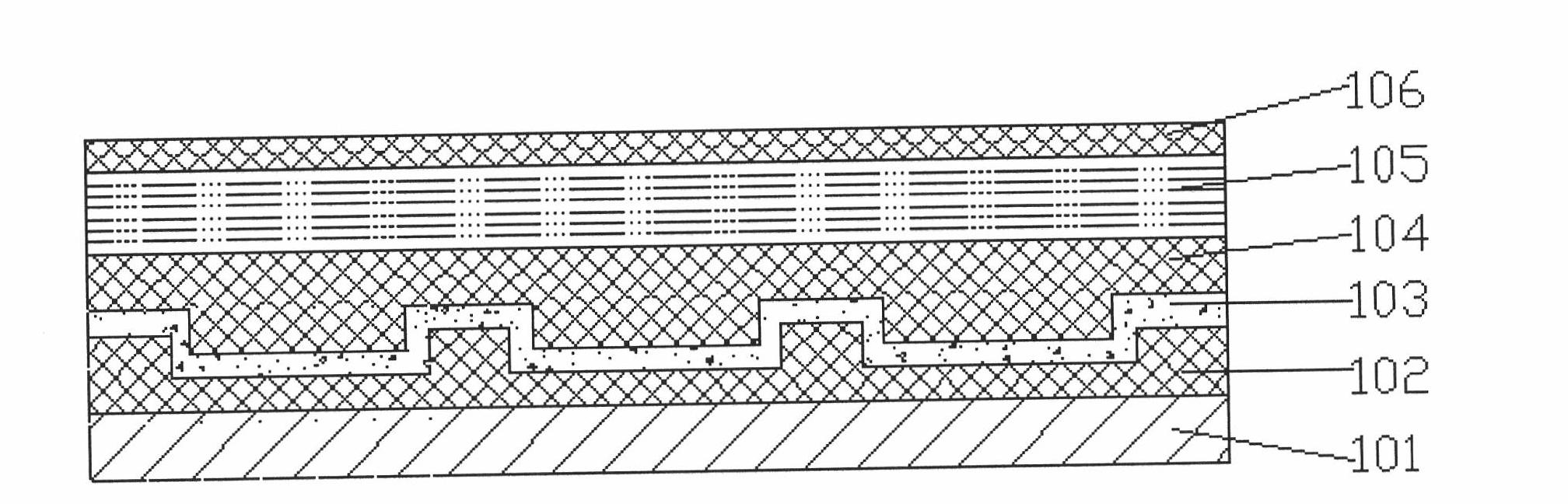
[0061] (1) select the glass substrate, adopt the PECVD method to deposit 1.0 micron low-temperature silicon oxide on the glass substrate as the barrier layer;

[0062] (2) Etching the barrier layer into a groove-shaped structure, wherein the protrusions have a rectangular cross-section, a width of 3 nanometers, a height of 3 nanometers (D=3.0nm), and a protrusion spacing of 60 microns;

[0063] (3) A layer of controllable nickel source is formed on the first isolation layer by sputtering as a metal induction layer, and the surface nickel concentration is 5×10 13 cm -2 ;

[0064] (4) Depositing a layer of barrier layer on the induction layer by PECVD method as the second barrier layer, the thickness of the second barrier layer corresponding to the protrusion of the first barrier layer is 1.5 nanomete...


PUM

PropertyMeasurementUnit
thicknessaaaaaaaaaa
thicknessaaaaaaaaaa
thicknessaaaaaaaaaa

Abstract

The invention provides a manufacturing method of a polycrystalline silicon film material, which is characterized by comprising the following steps of: 1. selecting a substrate, and forming a first blocking layer on the substrate; 2. sequentially forming a metal induced layer, a second blocking layer and an amorphous silicon layer on the first blocking layer; 3. carrying out primary annealing processing on a product obtained in step 2 to obtain a partially crystallized film; 4. forming a metal absorption layer on the partially crystallized film; 5. carrying out secondary annealing processing on the product obtained in step 2; and 6. removing the metal absorption layer after the secondary annealing processing. In the invention, the metal induced layer is formed before amorphous silicon and positioned between the two blocking layers, and because slot type structures are carved on the prepared blocking layers and have inconsistent and quite small distances with the amorphous silicon layer, the invention performs key actions on shortening the heat processing time, increasing the grain size and controlling and inducing metals to diffuse towards the amorphous silicon layer.

Description

technical field [0001] The invention belongs to the field of displays, in particular to a method for manufacturing polysilicon thin film materials used for manufacturing active matrix displays. Background technique [0002] At present, there are roughly two types of thin film transistor (TFT) technologies used in active matrix display devices: amorphous silicon thin film TFT and polysilicon thin film TFT. The amorphous silicon thin film TFT process is mature and relatively simple, with high yield and low cost. The characteristics of TFT are mainly evaluated by the value of electron mobility. The electron mobility of amorphous silicon thin film TFT is about 1cm2 / Vs and the stability of amorphous silicon devices is poor, which makes it difficult to meet the fast switching color sequential liquid crystal display, current-driven organic light-emitting diode display and other integrated display requirements. The electron mobility of polysilicon thin film TFT is about 100cm2 / Vs,...

Claims


Application Information

Patent Timeline
Patent Type & Authority Applications(China)
IPC IPC(8): H01L21/20H01L21/336
Inventor 彭俊华黄飚黄宇华
Owner GUANGDONG SINODISPLAY TECH
Why Eureka
Try Eureka