
Multispectral photoreceptive device and sampling method thereof

A photosensitive device and multi-spectral technology, applied in the direction of electric solid-state devices, semiconductor devices, electrical components, etc., can solve problems such as mediocrity and cramping

Active Publication Date: 2010-09-15
BOLY MEDIA COMM SHENZHEN
View PDF8 Cites 30 Cited by
  • Summary
  • Abstract
  • Description
  • Claims
  • Application Information

AI Technical Summary

Problems solved by technology

[0010] Especially, for the dual-layer or multi-layer photosensitive device that the present invention will pay attention to, the prior art just seems cramped and mediocre, because the dual-layer or multi-layer photosensitive device provides a lot of excellent color pattern arrangement, thus, whether it is Both signal reading and sub-sampling should be improved according to the characteristics of double-layer or multi-layer photosensitive devices

Method used


Image

  • Multispectral photoreceptive device and sampling method thereof
  • Multispectral photoreceptive device and sampling method thereof
  • Multispectral photoreceptive device and sampling method thereof

Examples


Embodiment Construction

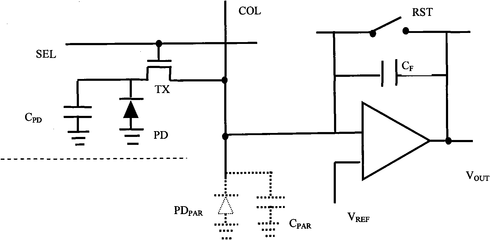
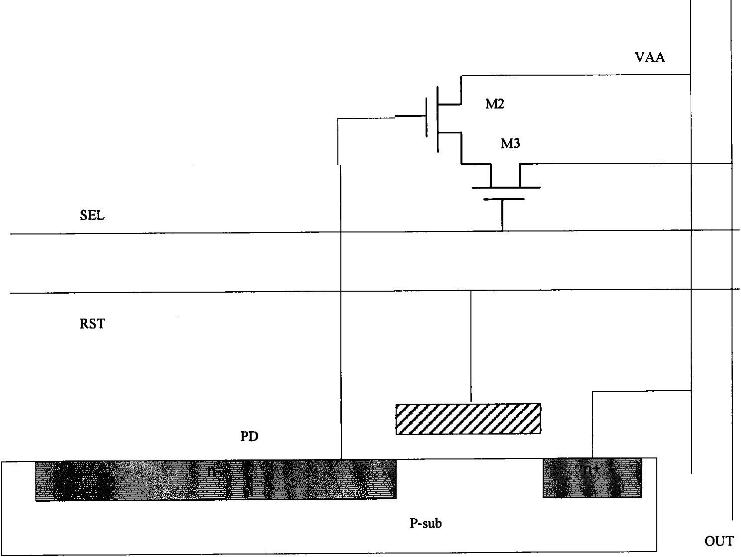
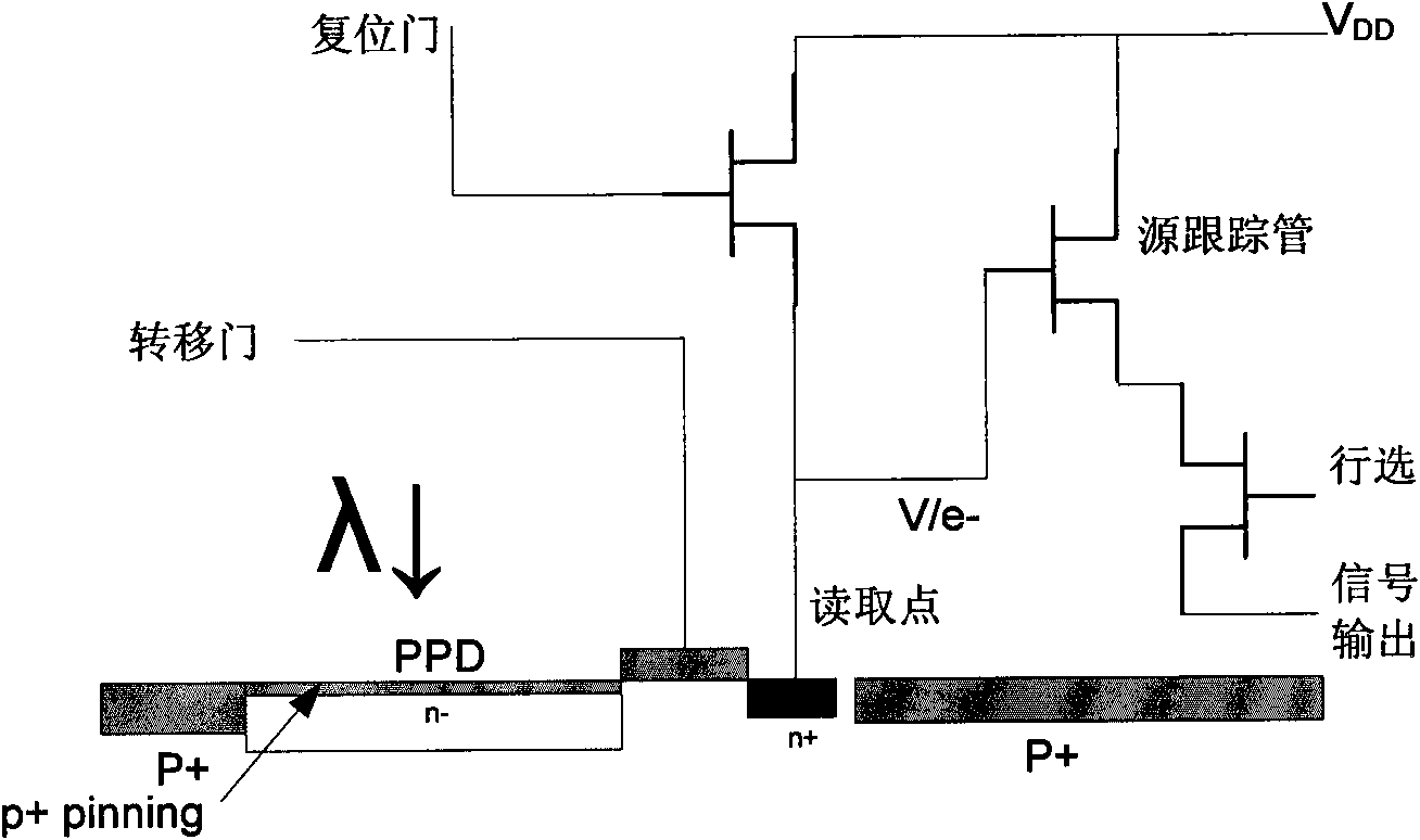
[0093] In the multi-spectral photosensitive device of the specific embodiment of the present invention, different reading and sub-sampling circuits can be composed of similar Figure 25 The circuit shown is implemented, including: a pixel array containing a plurality of macro pixels, a row address decoding controller, a column address decoding controller, a sampling control circuit, an amplification and an analog-to-digital conversion module, color conversion and sub-sampling, and an image processing module, output control module, chip total control module ( Figure 25 CC module in ), and possibly other modules.

[0094] According to needs, arrange the macro-pixels based on four-dot or three-dot pixels according to square matrix or honeycomb shape. These pixels can be passive pixels or active pixels, and can have a read capacitor FD or not have a read capacitor FD.

[0095] In the foregoing, we have distinguished the sub-sampling process into a first binning sampling process...


PUM


Abstract

The invention relates to a multispectral photoreceptive device and a sampling method thereof, wherein the method comprises the following processes that: a first merging process is used for pairwise merging and sampling among closely adjacent pixels in the same line and different columns, different lines and the same column or different lines and different columns in a pixel array and obtaining the sampling data of a first merged pixel; a second merging process is used for merging and sampling the sampling data of the first merged pixel obtained in the first merging process and obtaining the sampling data of a second merged pixel; and a third merging process is used for obtaining the sampling data of a third merged pixel in a digital space by color changing and image zooming methods. The invention is applicable for the multi-pixel sharing reading and amplifying circuit of a monolayer colored photoreceptive chip, a single-surface double-layer multispectral photoreceptive chip and a double-surface double-layer multispectral photoreceptive chip. On the basis of absorbing the kernel of a traditional pixel reading circuit, the invention has magnitude-order breakthrough on principles, basic circuits and performance and simply and directly realizes the YUV format output of sampled images on the photoreceptive device while realizing high-performance sub sampling.

Description

technical field [0001] The invention relates to the reading of photosensitive pixels of a photosensitive chip, especially the sub-sampling data reading of photosensitive pixels of a large array photosensitive chip. Specifically, the invention relates to a multi-spectrum photosensitive device and a sampling method thereof. Background technique [0002] The present invention is a continuation of "Multi-spectral photosensitive device and its manufacturing method" (PCT / CN2007 / 071262) and "Multi-spectral photosensitive device and its manufacturing method" (Chinese application number: 200810217270.2) earlier by the inventor, aiming at More specific and preferred semiconductor circuit and chip level implementations are provided. [0003] Previous photosensitive devices either focused on colored visible light or infrared light, and few combined the two. Although there are also other inventions or applications, such as semiconductor technology using cadmium indium ("Silicon infrare...

Claims


Application Information

Patent Timeline
IPC IPC(8): H04N3/15H04N9/04H01L27/14
Inventor 胡笑平
Owner BOLY MEDIA COMM SHENZHEN
Learn More