CMOS (Complementary Metal-Oxide Semiconductor) band-gap reference voltage generation circuit
A technology of reference voltage and circuit generation, applied in the fields of microelectronics and solid-state electronics, to achieve the effect of improving stability and eliminating the effect of second-order temperature modulation
- Summary
- Abstract
- Description
- Claims
- Application Information
AI Technical Summary
Problems solved by technology
Method used
Image
Examples
Embodiment Construction
[0021] Below in conjunction with accompanying drawing, the present invention is further elaborated.
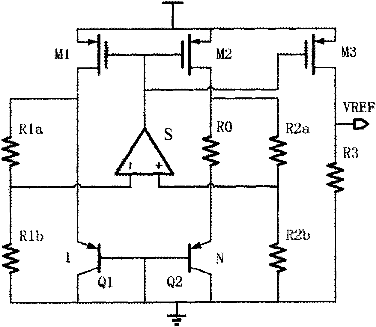
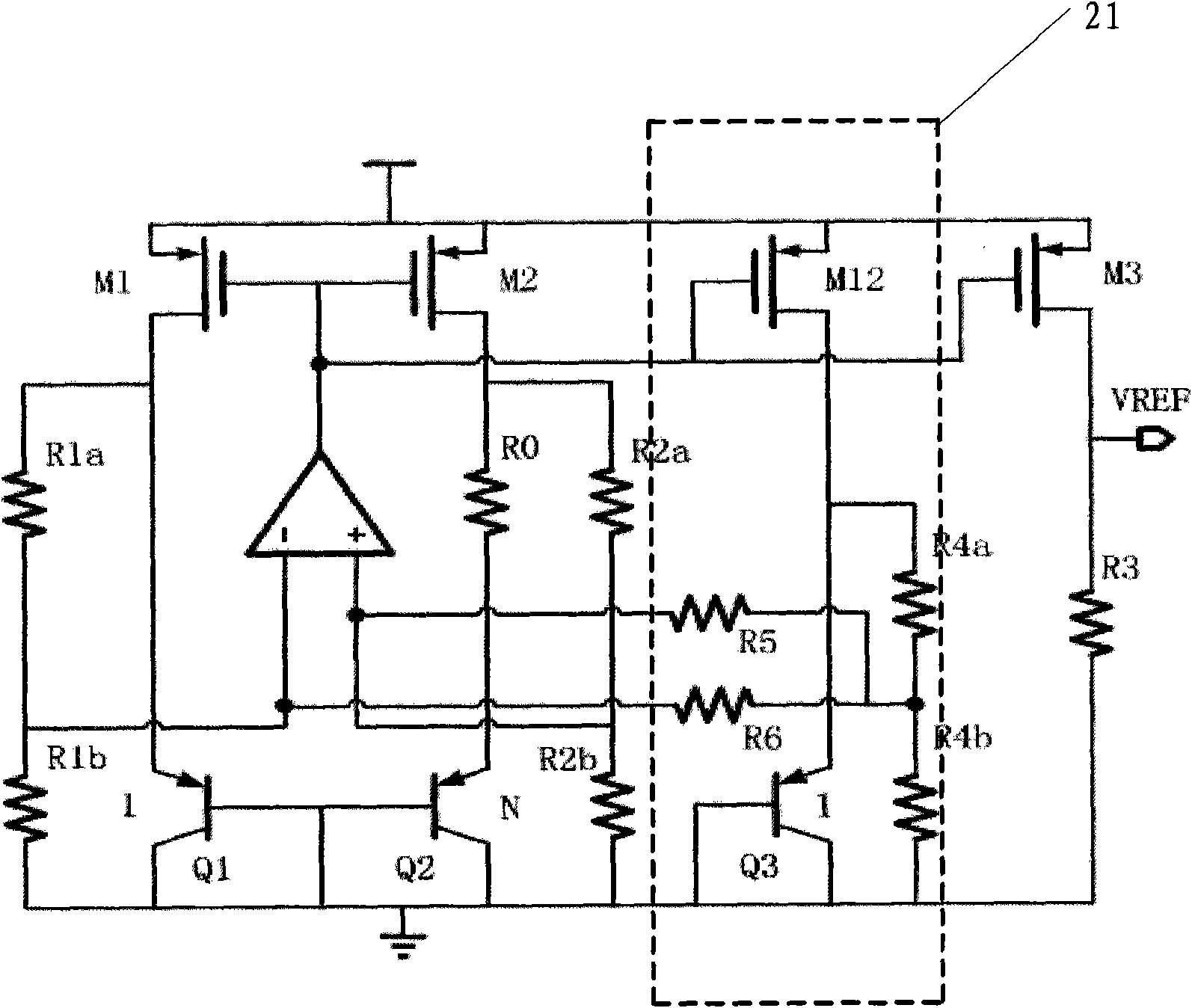
[0022] First, please refer to figure 2 , figure 2 It is a schematic structural diagram of the CMOS bandgap reference voltage generation circuit of the present invention, as can be seen from the figure, the present invention includes: a first CMOS M1, a second CMOS M2 and a third CMOS M3, the source of the first CMOS M1, The source of the second CMOS M2 is connected to the source of the third CMOS M3, the base of the first CMOS M1, the base of the second CMOS M2 and the base of the third CMOS M3 connected; the first transistor Q1 and the second transistor Q2, the collector and base of the first transistor Q1 and the collector and base of the second transistor Q2 are grounded, and the The emitter of the first transistor Q1 is connected to the drain of the first CMOS M1, the emitter of the second transistor Q2 is connected to the drain of the second CMOS M2; the amplifier S, ...
PUM
 Abstract
Description
Claims
Application Information


