Semiconductor device and method of manufacturing semiconductor device
A semiconductor and device technology, applied in the manufacture of semiconductor/solid-state devices, semiconductor devices, transistors, etc., can solve problems such as leakage voltage rise, and achieve the effect of suppressing current
- Summary
- Abstract
- Description
- Claims
- Application Information
AI Technical Summary
Problems solved by technology
Method used
Image

Examples
Embodiment Construction
[0034] Now, the present invention will be described herein with reference to exemplary embodiments. Those skilled in the art will recognize that many alternative embodiments can be accomplished using the teachings of the present invention and that the invention is not limited to the embodiments illustrated for explanatory purposes.
[0035] Hereinafter, referring to the drawings, embodiments of the present invention will be described. Note that any similar components in all drawings will be given similar reference numerals or symbols, and descriptions thereof will not be repeated all the time.
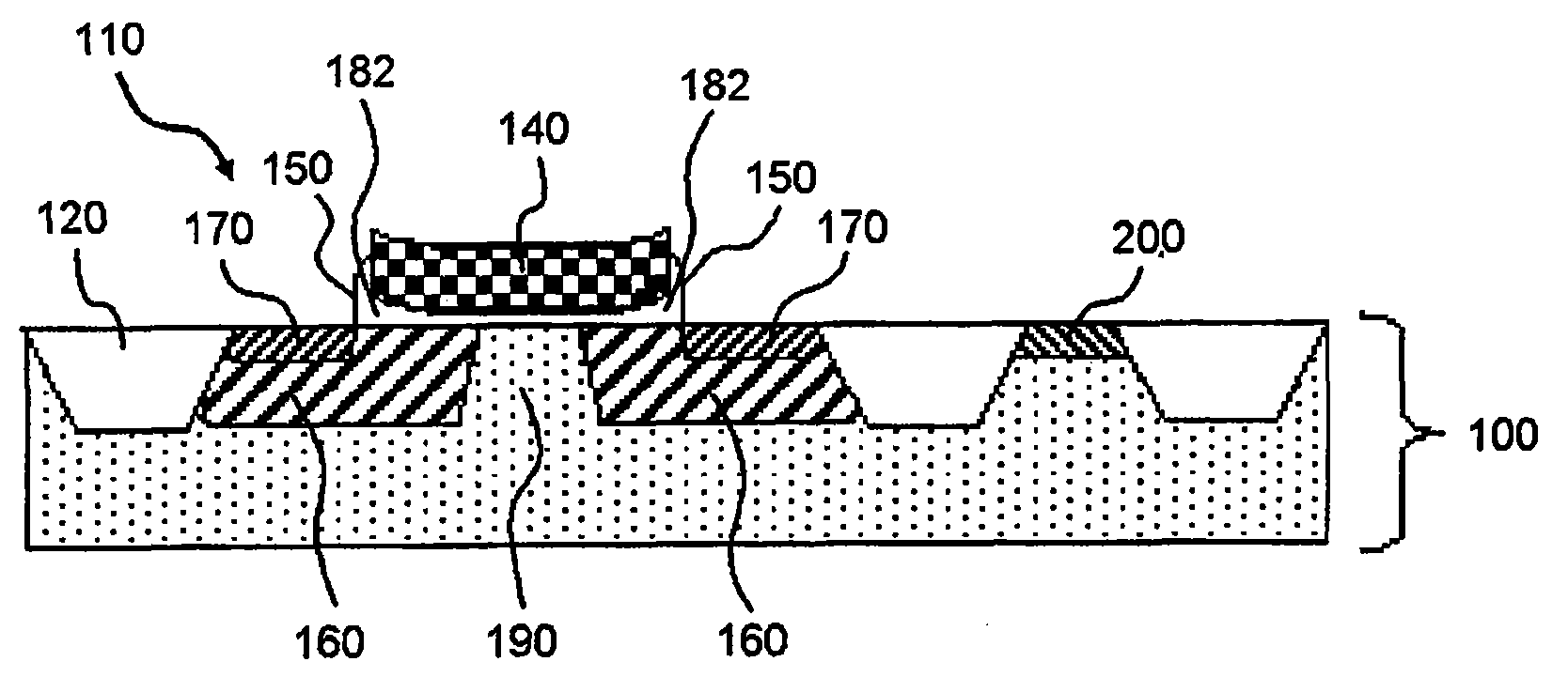
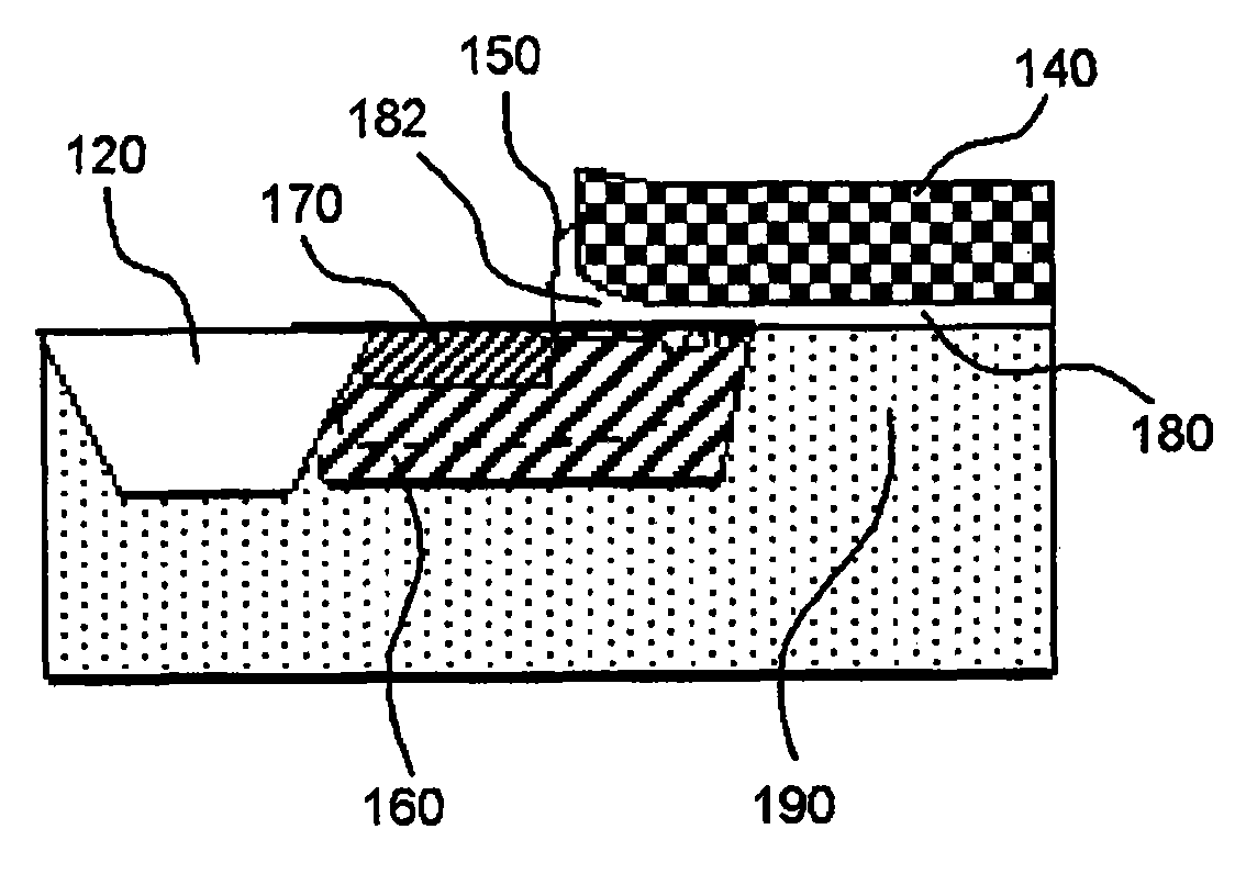
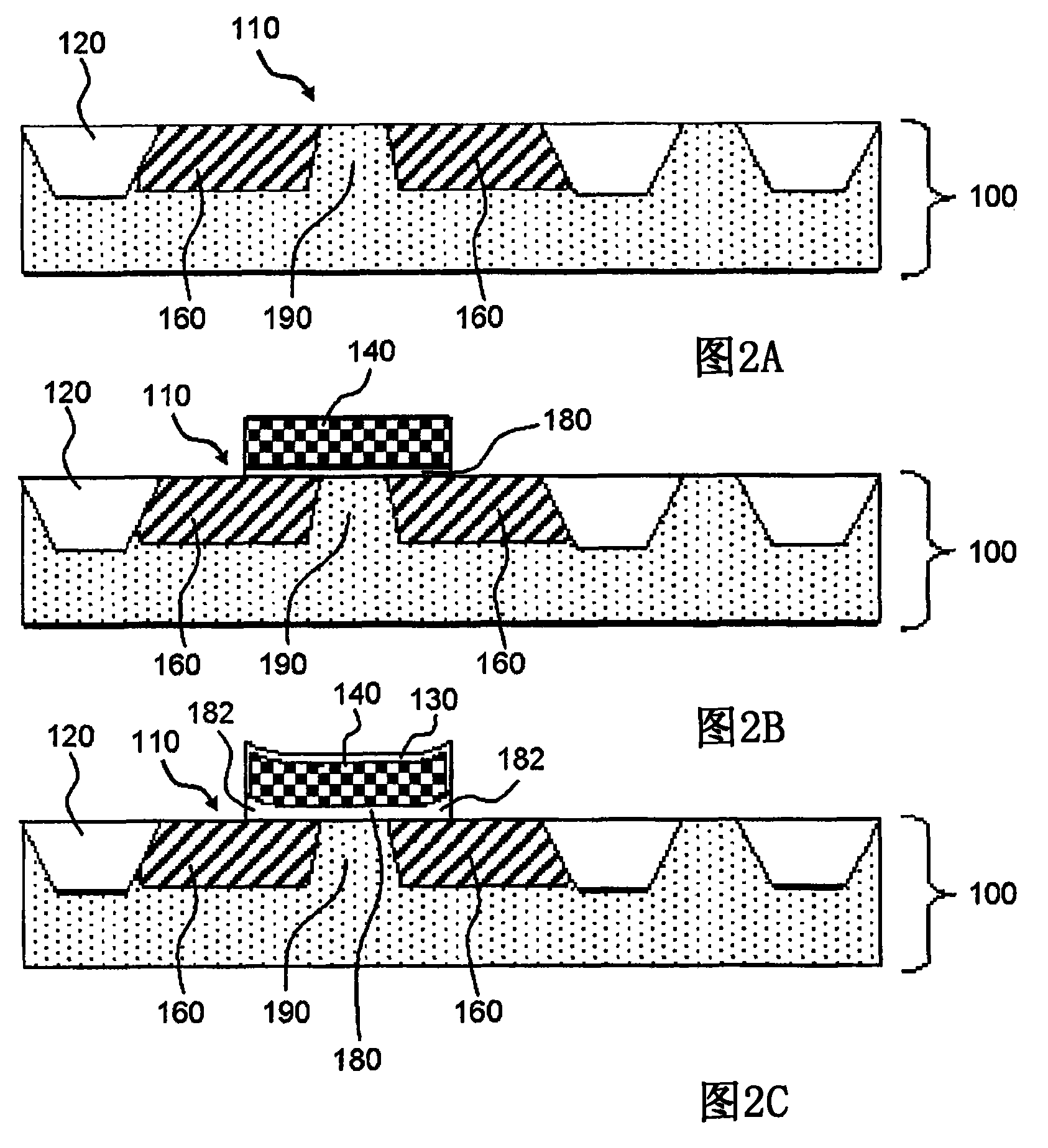
[0036] Figure 1A is a sectional view showing the semiconductor device according to the first embodiment; Figure 1B is showing Figure 1A A magnified view of the main part of . The semiconductor device has a device isolation film 120 formed in a semiconductor layer 100 of a first conductivity type, a device formation region 110, a channel formation region 190, a gate insulating fi...
PUM
| Property | Measurement | Unit |
|---|---|---|
| thickness | aaaaa | aaaaa |
Abstract
Description
Claims
Application Information
 - R&D
- Intellectual Property
- Life Sciences
- Materials
- Tech Scout
- Unparalleled Data Quality
- Higher Quality Content
- 60% Fewer Hallucinations
Browse by: Latest US Patents, China's latest patents, Technical Efficacy Thesaurus, Application Domain, Technology Topic, Popular Technical Reports.
© 2025 PatSnap. All rights reserved.Legal|Privacy policy|Modern Slavery Act Transparency Statement|Sitemap|About US| Contact US: help@patsnap.com