Composite film of inorganic insulating films and polyimide films used for three-pole field emission cathode

A technology of inorganic insulating film and polyimide film, applied in the direction of cathode ray tube/electron beam tube, discharge tube, electrical components, etc., can solve the problem that polyimide film is not suitable for insulating layer and polyimide insulating film Destruction, combined with poor reliability and other problems, to achieve large-area and cheap preparation, reduced chemical damage, and good insulation performance

Active Publication Date: 2013-04-17
FUZHOU UNIV
View PDF0 Cites 0 Cited by
  • Summary
  • Abstract
  • Description
  • Claims
  • Application Information

AI Technical Summary

Problems solved by technology

However, a single-layer polyimide film is not suitable as an insulating layer between the field emission cathode and the grid, including the following difficulties: First, the corrosion layer on the glass surface causes a gap between the polyimide and the glass substrate. The reliability of the combination is not good, and it may fall off; second, polyimide has the disadvantages of absorbing water and being dissolved and corroded by strong alkali, and it will cause damage to the polyimide insulating film when it is directly exposed to the subsequent wet etching liquid. Third, polyimide is susceptible to corona damage under the action of a strong electric field between the field emission cathode and grid

Method used


Image

  • Composite film of inorganic insulating films and polyimide films used for three-pole field emission cathode
  • Composite film of inorganic insulating films and polyimide films used for three-pole field emission cathode
  • Composite film of inorganic insulating films and polyimide films used for three-pole field emission cathode

Examples


Embodiment 1

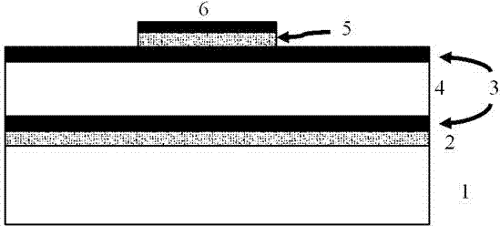
[0035] Using clean flat glass as the substrate, the metal grid is prepared by magnetron sputtering, photolithography and wet etching, and the material is Cr. Then reactive magnetron sputtering is used, and a mixed gas of Ar and O2 is used for sputtering to deposit a SiO2 layer with a thickness of about 100 nm. Use biphenyltetralic acid dianhydride and 4,4'-diaminodiphenyl ether with a purity of 99.99% as the dianhydride and diamine monomers of polyimide, dissolved in anhydrous N,N-dimethylformamide A polyamic acid solution with a solid content of 5% was formed in the solvent. The polyamic acid solution was spin-coated on top of the SiO2 layer at 80 o C bake for 2 hours, then respectively at 120 o C. 160 o C. 200 o C. 260 o C. 300 o C heat treatment for 30 minutes, then raised to 350 o C. 400 o C and 450 o Each of C was kept warm for 10 minutes, and finally cooled naturally to take it out to complete the imidization treatment, and the thickness of the polyimide film wa...

Embodiment 2

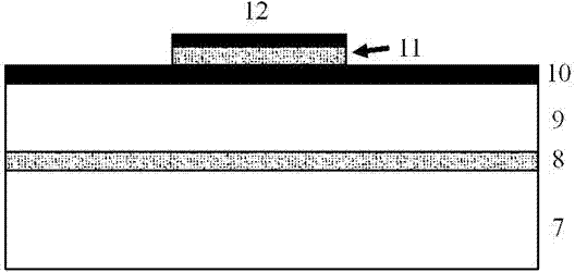
[0038] Using clean flat glass as the substrate, the metal grid is prepared by magnetron sputtering, photolithography and wet etching, and the material is Cr. Then reactive magnetron sputtering is used, and a mixed gas of Ar and N2 is used for sputtering to deposit a Si3N4 layer with a thickness of about 100 nm. Use biphenyltetralic acid dianhydride and 4,4'-diaminodiphenyl ether with a purity of 99.99% as the dianhydride and diamine monomers of polyimide, dissolved in anhydrous N,N-dimethylformamide A polyamic acid solution with a solid content of 5% was formed in the solvent. The polyamic acid solution was spin-coated on the Si3N4 layer, 80 o C bake for 2 hours, then respectively at 120 o C. 160 o C. 200 o C. 260 o C. 300 o C heat treatment for 30 minutes, then raised to 350 o C. 400 o C and 450 o Each of C was kept warm for 10 minutes, and finally cooled naturally to take it out to complete the imidization treatment, and the thickness of the polyimide film was 3 μm....

Embodiment 3

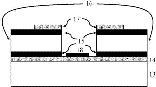
[0041] Using clean flat glass as the substrate, the gate electrode is prepared by magnetron sputtering, photolithography and wet etching, and the material is Cr. Use biphenyltetralic acid dianhydride and 4,4'-diaminodiphenyl ether with a purity of 99.99% as the dianhydride and diamine monomers of polyimide, dissolved in anhydrous N,N-dimethylformamide A polyamic acid solution with a solid content of 5% was formed in the solvent. The polyamic acid solution was sprayed on the glass substrate, 80 o C bake for 2 hours, then respectively at 120 o C. 160 o C. 200 o C. 260 o C. 300 o C heat treatment for 30 minutes, then raised to 350 o C. 400 o C and 450 o C each keep warm for 10 minutes, and finally take it out by natural cooling to complete the imidization treatment, and the thickness of the polyimide film is 4 μm. On the polyimide film, a SiO2 film with a thickness of 200nm was prepared by reactive magnetron sputtering, and then a Cr cathode electrode metal film was depo...


PUM

PropertyMeasurementUnit
thicknessaaaaaaaaaa
thicknessaaaaaaaaaa
thermal decomposition temperatureaaaaaaaaaa

Abstract

The invention provides a structure of a composite insulating film with organic and inorganic laminations and a preparation method thereof, which are used for a field emission flat plate display. The composite insulating film is formed by superposing inorganic insulating films and polyimide films, and the arrangement mode of the inorganic insulating films and the polyimide films in the composite insulating film along a direction from a field emission cathode substrate to an anode is: the inorganic insulating film, the polyimide film, the inorganic insulating film or the polyimide film, and theinorganic insulating film. In the direction from a field emission cathode to the anode, the structure of the field emission cathode substrate comprises a glass substrate, a grid electrode, the composite insulating film and the field emission cathode, or the glass substrate, the field emission cathode, the composite insulating film and the grid electrode. By adopting the composite insulating film to construct a front grid or back grid structure, a large area of reliable insulation between the cathode and the grid electrode on the field emission flat plate display can be obtained in a low-pricemode.

Description

technical field [0001] The invention provides a structure and a preparation method of an organic-inorganic lamination composite insulating film, which are used for a field emission flat panel display. Background technique [0002] Field Emission Flat Panel Display (FED) is a new type of flat panel display technology that combines the advantages of both CRT and LCD. The principle of FED is to apply a strong electric field near the field emission cathode, so that the field emission cathode can emit electrons, and the electrons are accelerated by the anode voltage and bombard the phosphor on the anode to emit light. Composing the field emission cathode unit and the corresponding anode unit into a flat plate array, the electron emission current density of the field emission unit can be controlled by adjusting the electric field intensity on each field emission cathode unit, thereby realizing the brightness control of the anode unit, and Realize the display of images and videos....

Claims


Application Information

Patent Timeline
Patent Type & Authority Patents(China)
IPC IPC(8): H01J29/02H01J29/08
Inventor 袁军林翁卫祥于光龙郭太良
Owner FUZHOU UNIV
Why Eureka
Try Eureka