Solder pad and packaging structure applying same
A packaging structure and welding pad technology, which is applied in the direction of electrical components, electrical solid devices, circuits, etc., can solve problems that affect the electrical function of the chip packaging structure and poor quality
- Summary
- Abstract
- Description
- Claims
- Application Information
AI Technical Summary
Problems solved by technology
Method used
Image

Examples
no. 1 example
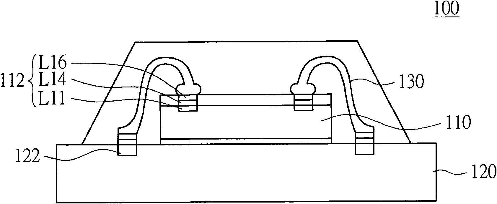
[0026] Please refer to figure 1 , which is a schematic diagram of the packaging structure 100 according to the first embodiment of the present invention. The packaging structure 100 includes a first semiconductor device 110 , a second semiconductor device 120 and a bonding wire 130 . In this embodiment, the first semiconductor component 110 is, for example, a die. The second semiconductor device 120 is, for example, a substrate, a wafer or a lead frame. In this embodiment, the second semiconductor component 120 is described by taking a substrate as an example. The first semiconductor component 110 includes at least one pad 112 . The second semiconductor component 120 includes at least one pad 122 . One end of the bonding wire 130 is soldered to the bonding pad 112 of the first semiconductor component 110 , and the other end of the bonding wire 130 is soldered to the bonding pad 122 of the second semiconductor component 120 . Through the connection of the bonding wire 130 ...
no. 2 example
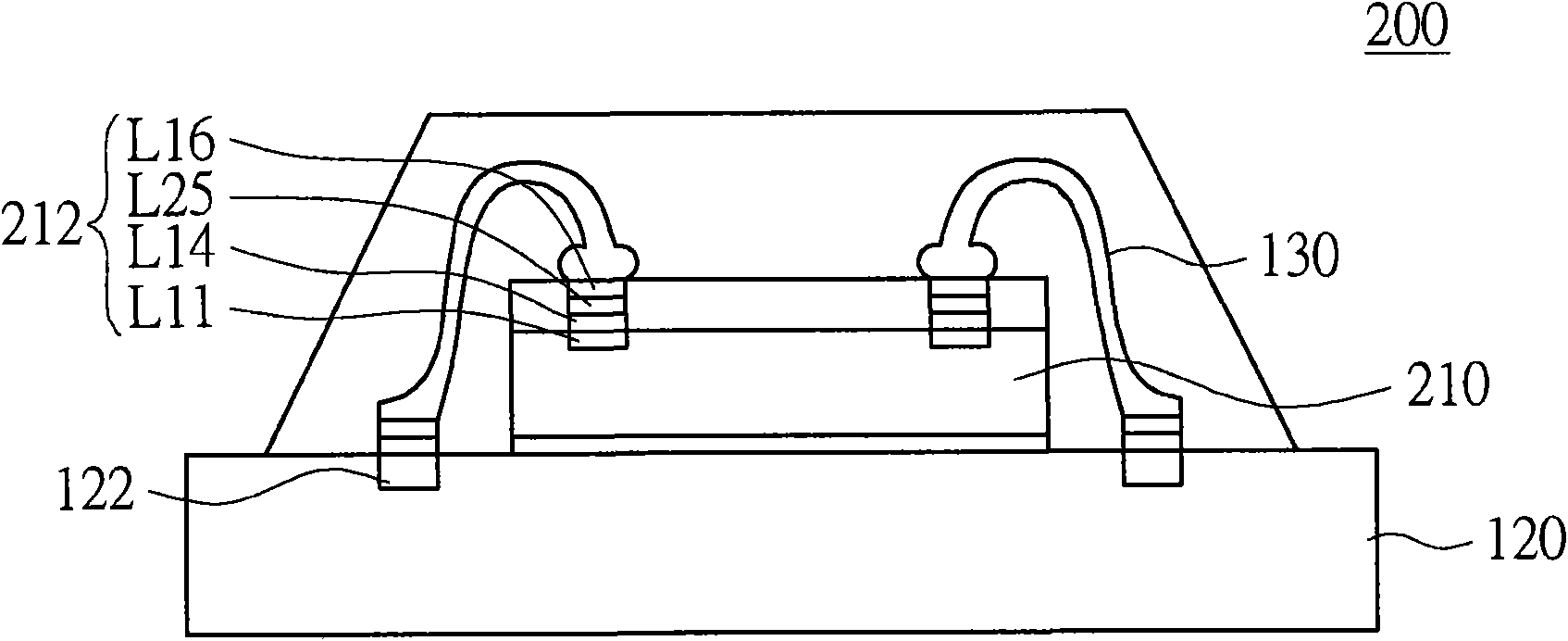
[0036] Please refer to figure 2 , which is a schematic diagram of the packaging structure 200 according to the second embodiment of the present invention. The difference between the package structure 200 of this embodiment and the package structure 100 of the first embodiment is that the bonding pad 212 of the first semiconductor device 210 further includes an anti-oxidation metal layer L25 , and the rest of the similarities will not be described again.
[0037] like figure 2 As shown, the anti-oxidation metal layer L25 is disposed between the hard metal layer L14 and the anti-oxidation metal layer L16. The activity of the material of the anti-oxidation metal layer L25 is also lower than that of the material of the hard metal layer L14. In this embodiment, an anti-oxidation metal layer L25 is added between the hard metal layer L14 and the anti-oxidation metal layer L16, which can not only increase the anti-oxidation effect, but also increase the bonding effect between the ...
no. 3 example
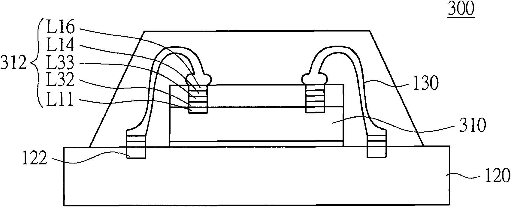
[0044] Please refer to image 3 , which is a schematic diagram of a packaging structure 300 according to a third embodiment of the present invention. The package structure 300 of this embodiment is different from the package structure 100 of the first embodiment in that the bonding pad 312 of the first semiconductor component 310 of this embodiment further includes a seed layer L32 and a conductive layer L33, and the rest are the same, without Repeat the narrative again.
[0045] like image 3 As shown, the seed layer L32 is disposed on the metal substrate L11, and the conductive layer L33 is disposed between the seed layer L32 and the hard metal layer L14. In this embodiment, a seed layer L32 and a conductive layer L33 are added between the metal substrate L11 and the hard metal layer L14, which not only increases the convenience of forming the hard metal layer L14 by electroplating, but also increases the contact between the hard metal layer L14 and the metal layer. Bondi...
PUM
| Property | Measurement | Unit |
|---|---|---|
| thickness | aaaaa | aaaaa |
| thickness | aaaaa | aaaaa |
| thickness | aaaaa | aaaaa |
Abstract
Description
Claims
Application Information