Etch resistant wafer processing apparatus and method for producing the same

a technology of processing apparatus and etching resistance, which is applied in the direction of turning machine accessories, chucks, baking ovens, etc., can solve the problems of low thermal shock resistance, limiting the maximum ramp to approximately 12 to 20° c, and generating backside particles becomes a serious problem

Inactive Publication Date: 2007-06-21
MOMENTIVE PERFORMANCE MATERIALS INC
View PDF4 Cites 35 Cited by
  • Summary
  • Abstract
  • Description
  • Claims
  • Application Information

AI Technical Summary

Problems solved by technology

The semiconductor wafer is heated within a confined environment in a processing vessel at relatively high temperature and often in an atmosphere, which is highly corrosive.
A well-known problem with the sintered AlN etch resistant heaters o

Method used


Image

  • Etch resistant wafer processing apparatus and method for producing the same
  • Etch resistant wafer processing apparatus and method for producing the same
  • Etch resistant wafer processing apparatus and method for producing the same

Examples


example 1

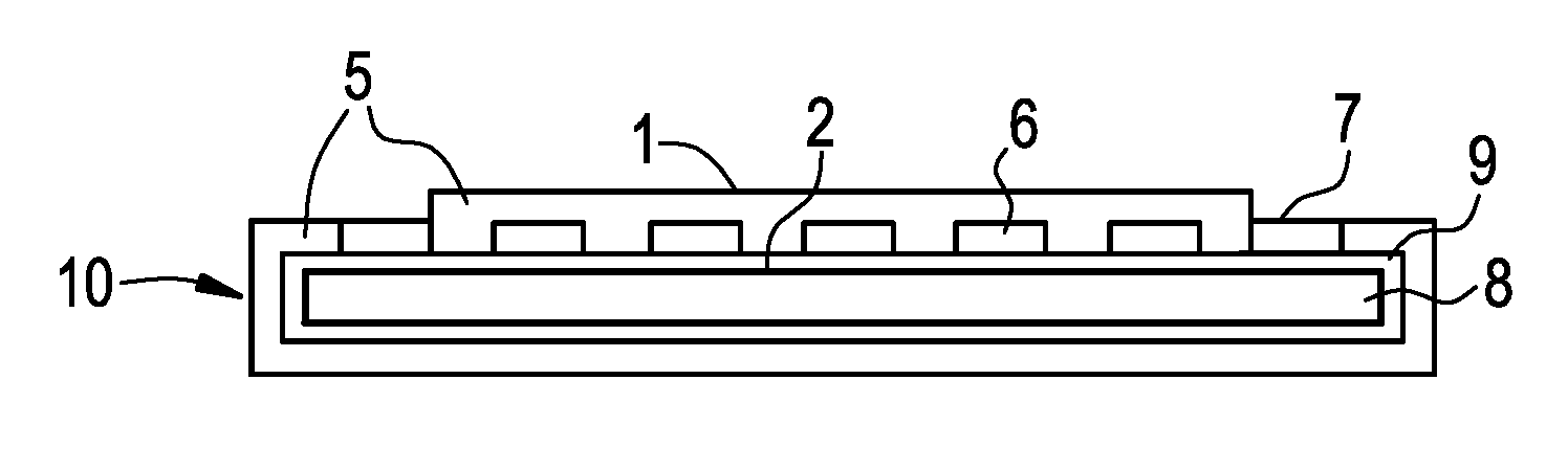
[0063] A heater having the architecture illustrated in FIG. 1 was produced with a 4″ diameter sintered AlN disk having a thickness of 0.125″ as the base substrate reference. Screen printed Mo-Mn (30% frit) electrodes were printed onto the substrate for a film thickness of 50 μm. The structure was coated with a layer of CVD AlN of a thickness of 50 to 100 μm. The CVD process to form AlN coatings was conducted in a furnace at a temperature of about 1000° C., wherein Cl2 flow in the range of 1-3 slm was passed through hot Al bars at about 350 to 500° C., and further mixed with NH3 at a flow rate of 1-10 slm, N2 of 5-8 slm, and H2 of 0.8-5 slm.

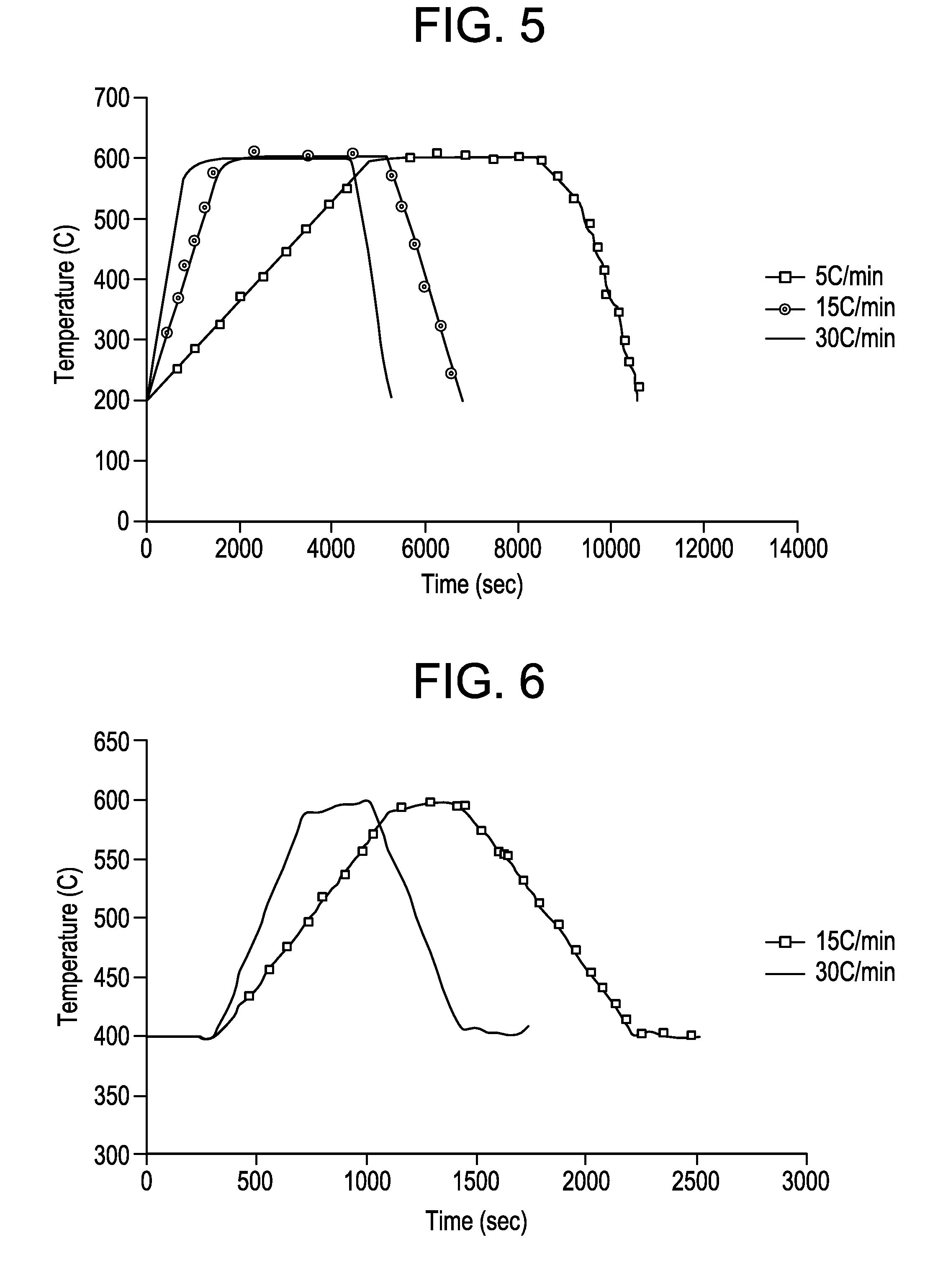
[0064] The disk heater was powered to cycle between 200° C. to 600° C. with ramp rates from 5° C., 15° C., and 30° C. The heater demonstrated excellent thermal shock resistance and mechanical integrity even after the heating tests. However, during rapid heating, it was observed that if the contacts were noticeably cooler than the center (a differ...

example 2

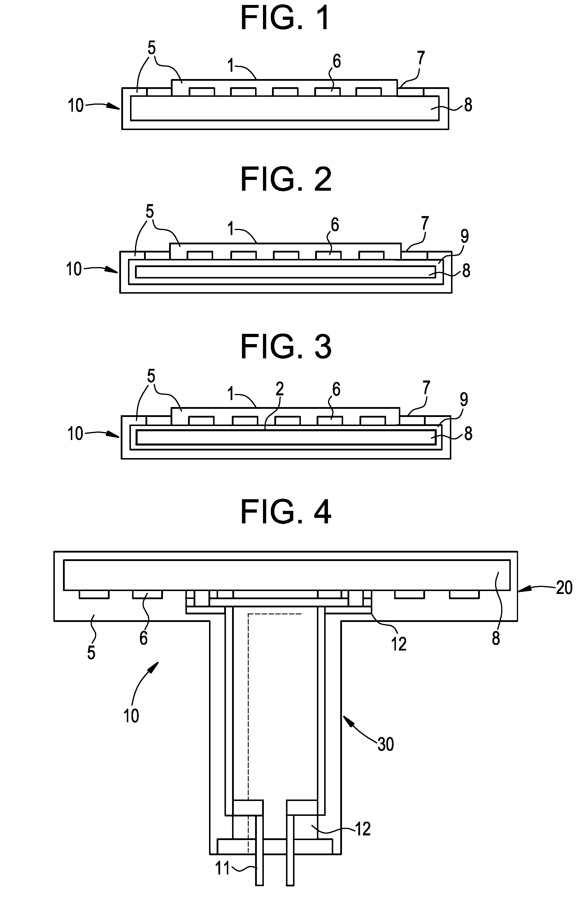
[0066] A heater having the architecture illustrated in FIG. 2 was produced with a 4″ diameter disk having a graphite core having a thickness of 0.25″, and a CVD AlN coating layer of a thickness of 100 to 200 μm as the base substrate. A 10 μm thick TaC tie layer was used between the CVD AlN layer and the graphite core. Screen printed Mo—Mn (30% frit) electrodes were printed onto those substrates for a film thickness of 50 μm, and final-coated by another layer of CVD AlN with a film thickness of 50 to 100 μm. The prototype disk heater was powered to cycle between 400° C. to 600° C. with ramp rates from 15° C. to 30° C. The CVD process to coat AlN was the same as in Example 1.

[0067]FIG. 6 is a graph showing the results of the ramp test, showing that the heater ramps up quickly in a short period of time, while still maintaining excellent thermal shock resistance and mechanical integrity. Multiple thermal life cycles were performed, demonstrating the outstanding reliability of such arch...


PUM

PropertyMeasurementUnit
Temperatureaaaaaaaaaa
Percent by massaaaaaaaaaa

Abstract

A wafer processing apparatus is fabricated by depositing a film electrode onto the surface of a base substrate, the structure is then overcoated with a protective coating film layer comprising at least one of a nitride, carbide, carbonitride or oxynitride of elements selected from a group consisting of B, Al, Si, Ga, refractory hard metals, transition metals, and combinations thereof. The film electrode has a coefficient of thermal expansion (CTE) that closely matches the CTE of the underlying base substrate layer as well as the CTE of the protective coating layer.

Description

CROSS REFERENCE TO RELATED APPLICATION [0001] This application claims priority of U.S. Application No. 60 / 752,677, filed on Dec. 21, 2005, and U.S. patent application Ser. No. 10 / 875,861, filed on Jun. 25, 2003, which patent applications are fully incorporated herein by reference.FIELD OF INVENTION [0002] The invention relates generally to a wafer handling apparatus for use in the manufacture of semiconductors. BACKGROUND OF THE INVENTION [0003] Wafer handling apparatuses, e.g., heaters and electrostatic chucks (“ESC”), are used in a number of system applications such as molecular beam epitaxy, space experiments, substrate heaters for electron microscopy and in the growth of superconducting films, etc. A wafer handling assembly may include a susceptor for supporting a wafer, and a plurality of heaters disposed under the susceptor to heat the wafer. The semiconductor wafer is heated within a confined environment in a processing vessel at relatively high temperature and often in an at...

Claims


Application Information

Patent Timeline
IPC IPC(8): H01L23/58
CPCH01L21/67011H01L21/67103Y10T279/23Y10S269/903H01L21/68757H01L21/02
Inventor FAN, WEISANE, AJITLENNARTZ, JEFFREYKIM, TAE WON
Owner MOMENTIVE PERFORMANCE MATERIALS INC
Why Eureka
Try Eureka