Alternating current light-emitting device

A light-emitting device and light-emitting layer technology, which is applied in the direction of lighting devices, electroluminescent light sources, light sources, etc., can solve the problems of limiting the effective light-emitting area of ​​the light-emitting device, failing to emit light, and rectifying circuits that cannot operate

Inactive Publication Date: 2010-10-13
宁波璨圆光电有限公司
View PDF4 Cites 3 Cited by
  • Summary
  • Abstract
  • Description
  • Claims
  • Application Information

AI Technical Summary

Problems solved by technology

[0004] However, the plurality of first light-emitting units 142 of the first light-emitting module 14 and the plurality of second light-emitting units 162 of the second light-emitting module 16 each occupy half of the area of ​​the substrate 12, so the existing AC light-emitting devices 10 respectively operate under positive and negative conditions of the alternating current. The light-emitting area in the negative half-wave cycle is only half, so the existing AC light-emitting device 10 can only provide the original light-emitting efficiency of the existing AC light-emitting device 10 due to the light-emitting area provided by the first light-emitting module 14 and the second light-emitting module 16 half of that, and the plurality of first light emitting units 142 and the plurality of second light emitting units 162 of the existing AC light emitting device 10 only use one wire 144, 164 to couple the polarity of the power supply to the adjacent light emitting units, therefore When one of the wires 144, 164 is disconnected, one of the first light emitting module 14 and the second light emitting module 16 of the existing AC light emitting device 10 will be open and unable to emit light, thus causing the existing AC light emitting device to 10 can only emit light in one of the p

Method used


Image

  • Alternating current light-emitting device
  • Alternating current light-emitting device
  • Alternating current light-emitting device

Examples


Embodiment Construction

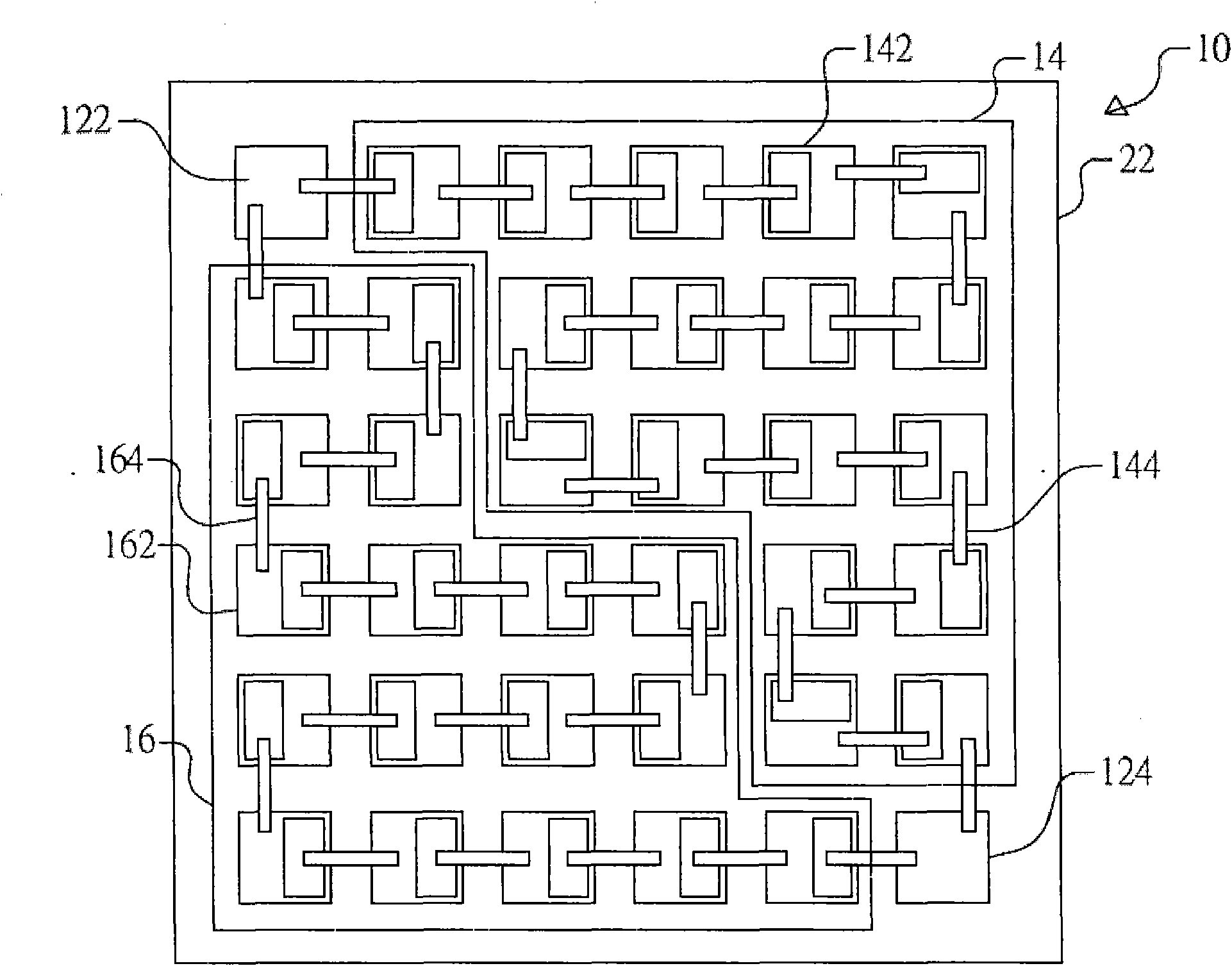
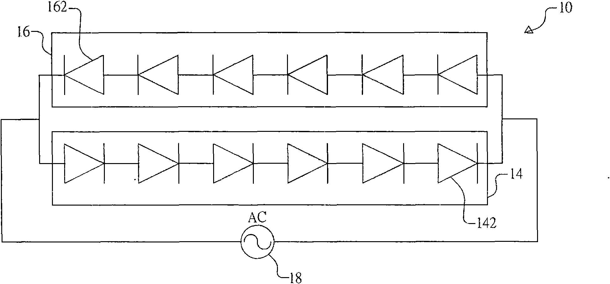
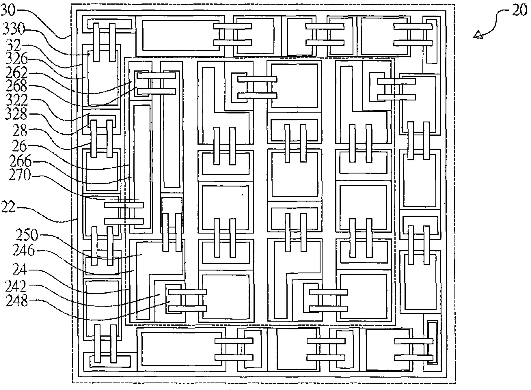
[0033] see Figure 2A to Figure 2C , shows a top view and a schematic structural view of an AC light emitting device according to an embodiment of the present invention. Such as Figure 2A As shown, the present embodiment is an AC light emitting device 20, which includes a substrate 22, a plurality of first light emitting units 24, a plurality of second light emitting units 26 and a plurality of wires 28, the plurality of first light emitting units 24 and the plurality of light emitting units A plurality of second light-emitting units 26 are respectively arranged on the substrate 22, and the areas of the plurality of first light-emitting units 24 and the plurality of second light-emitting units 26 are different, wherein the plurality of first light-emitting units 24 and The plurality of second light-emitting units 26 are semiconductor epitaxial layers, and the plurality of first light-emitting units 24 are respectively coupled to adjacent light-emitting units through the firs...


PUM


Abstract

The invention discloses an alternating current (AC) light-emitting device. The device comprises a substrate and a plurality of light-emitting units, wherein the light-emitting units are arranged on the substrate, each light-emitting unit contains a first semiconductor layer, a luminous layer and a second semiconductor layer from bottom to top, at least one first electrode and second electrode are separately arranged on the first semiconductor layer and the second semiconductor layer, and each light-emitting unit is coupled with at least one adjacent light-emitting unit through a wire. As the light-emitting device has a plurality of light-emitting units and each light-emitting unit is coupled with at least one adjacent light-emitting unit through a wire, the problem that as one wire is broken, the AC light-emitting device is open can be avoided.

Description

technical field [0001] The invention relates to a light emitting device, in particular to an AC light emitting device. Background technique [0002] Light Emitting Diode (LED) is a light-emitting component made of semiconductor materials. The component has a voltage applied between two electrodes, and a very small current is passed through. The form is stimulated to release, which is the basic principle of light-emitting diodes. Light-emitting diodes are different from ordinary incandescent light bulbs. Light-emitting diodes are cold-emitting, and have the advantages of low power consumption, long component life, no warm-up time, and fast response. In addition, they are small in size, resistant to vibration, suitable for mass production, and easy to use. According to the requirements of the application, it can be made into extremely small or array components. At present, light-emitting diodes have been widely used in indicators and display devices of information, communicat...

Claims


Application Information

Patent Timeline
IPC IPC(8): H05B33/12H05B33/26
Inventor 冯辉庆黄国钦潘锡明潘宏立
Owner 宁波璨圆光电有限公司
Why Eureka
Try Eureka