Photoelectric conversion element and solar cell
A photoelectric conversion element, a general-type technology, applied in the direction of electrical components, photovoltaic power generation, electrolytic capacitors, etc., can solve the problem of low conversion efficiency, and achieve the effect of good adsorption and high photoelectric conversion efficiency
Inactive Publication Date: 2010-10-20
KONICA MINOLTA BUSINESS TECH INC
18 Cites 10 Cited by
AI-Extracted Technical Summary
Problems solved by technology
However, even when these dyes are used, the conversion efficiency is lower than when a ruthenium c...
Abstract
Provided is a photoelectric conversion element for which a novel compound (dye) exhibiting excellent adsorption to an oxide semiconductor and exhibiting high photoelectric conversion efficiency is used, and also provided is a solar cell employing the photoelectric conversion element. Disclosed is a dye-sensitizing type photoelectric conversion element possessing at least a pair of facing electrodes, a semiconductor layer possessing a semiconductor and a sensitizing dye supported on the semiconductor, and a charge transport layer, wherein the semiconductor layer and the charge transport layer are provided between the facing electrodes, and wherein the sensitizing dye comprises a compound represented by the following Formula (1).
Application Domain
Styryl dyesElectrolytic capacitors +7
Technology Topic
Oxide semiconductorEngineering +8
Image
Examples
- Experimental program(3)
Example Embodiment
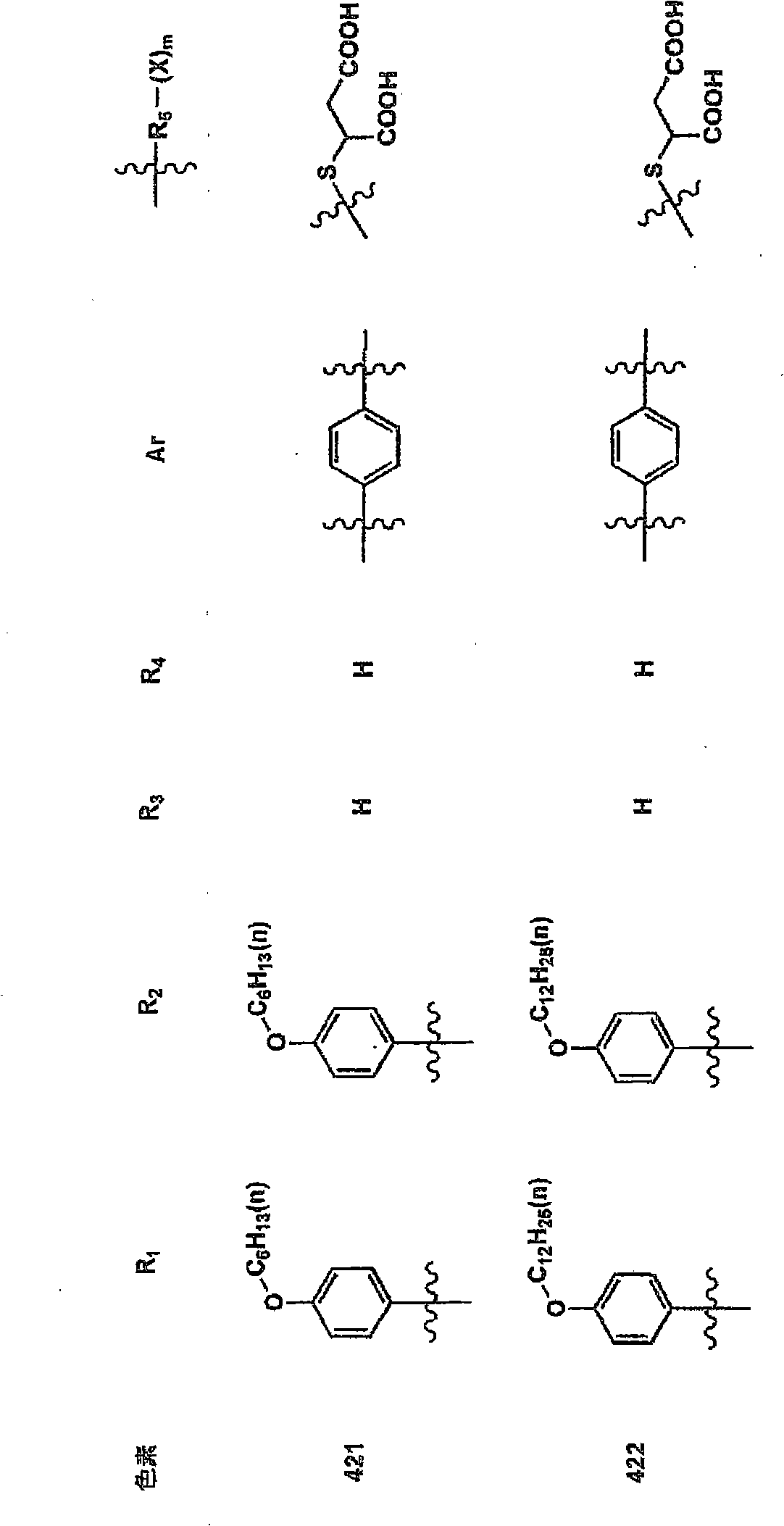
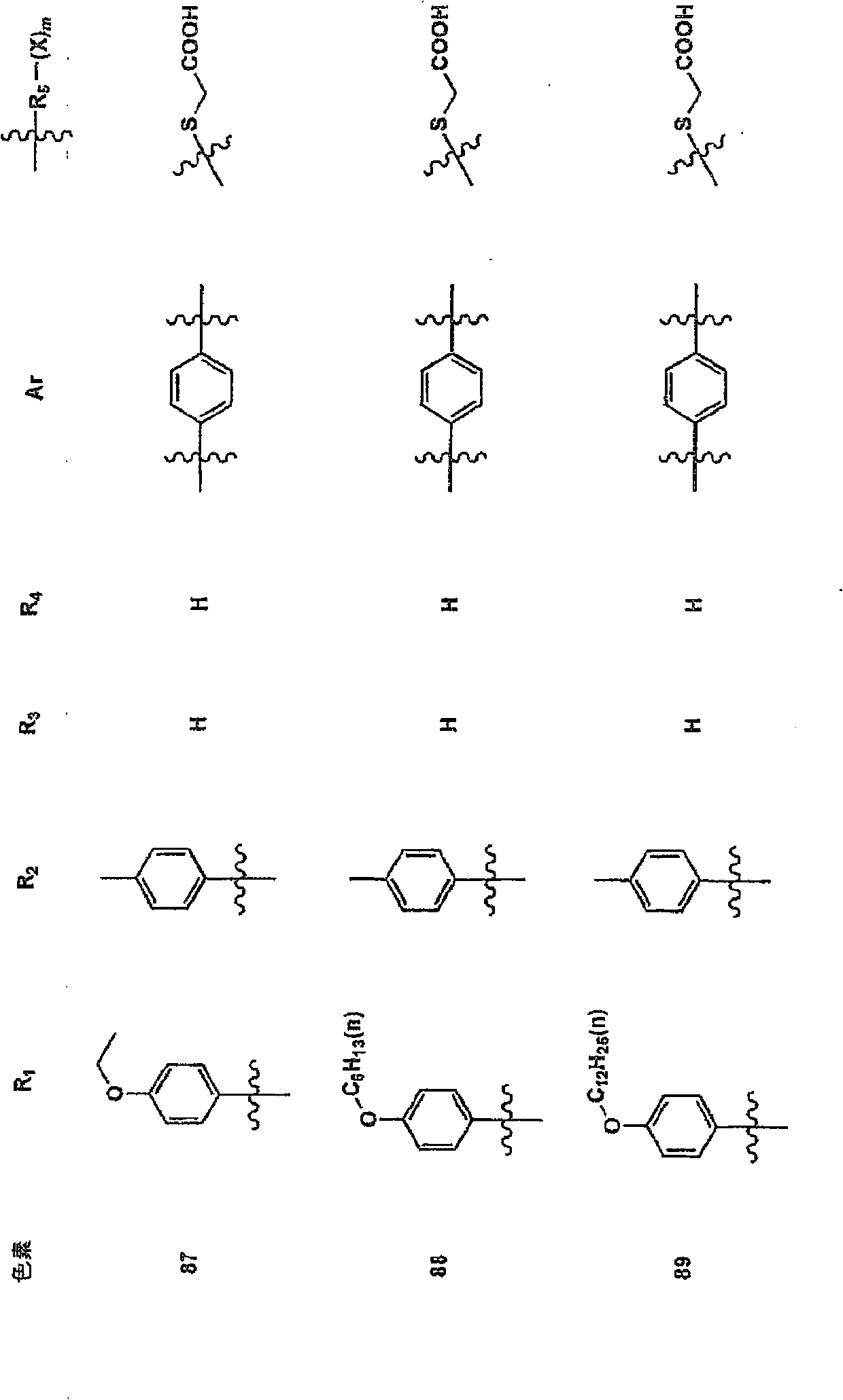
Synthesis Example 1 (Synthesis of Pigment 1)
The aldehyde (compound A) was added to a DMF solution of 2.5 equivalents of diethyl benzhydryl phosphonate and 3 equivalents of K-OtBu, and stirred at 120°C for 1 hour. After adding water to the reaction solution, it was extracted with ethyl acetate, washed with water, dried with magnesium sulfate, concentrated to dryness with a rotary evaporator, and treated with a silica column to obtain compound B.
1.5 equivalents of phosphorus oxychloride and 3 equivalents of DMF were added to the toluene solution of compound B, and stirred at 60°C for 1 hour. Cold water was added to the reaction solution, stirred at room temperature for 1 hour, extracted with ethyl acetate, washed with water, dried with magnesium sulfate, concentrated and dried with a rotary evaporator, and treated with a silica column to obtain compound C .
The acetic acid solution containing compound C, 1.2 equivalents of thiohydantoin, and 3 equivalents of ammonium acetate was stirred at 120°C for 1 hour. After adding water to the reaction solution, it was extracted with ethyl acetate, washed with water, dried with magnesium sulfate, concentrated to dryness with a rotary evaporator, and treated with a silica column to obtain compound D.
1.05 equivalents of bromoacetic acid and 3 equivalents of potassium hydroxide were added to the ethanol solution of compound D, and the mixture was stirred at 70°C for 1 hour. After concentrating and drying with a rotary evaporator, water and ethyl acetate were added, and the organic layer was removed with a separatory funnel. An excess of 1mol/l hydrochloric acid was added to the water layer, stirred for 5 minutes, extracted with ethyl acetate, washed with water, dried with magnesium sulfate, concentrated to dryness with a rotary evaporator, and treated with a silica column to obtain Pigment 1.
For pigment 1, the structure was confirmed by nuclear magnetic resonance spectroscopy and mass spectrometry.
"semiconductor"
Compound B
Compound C
"semiconductor"
Example Embodiment
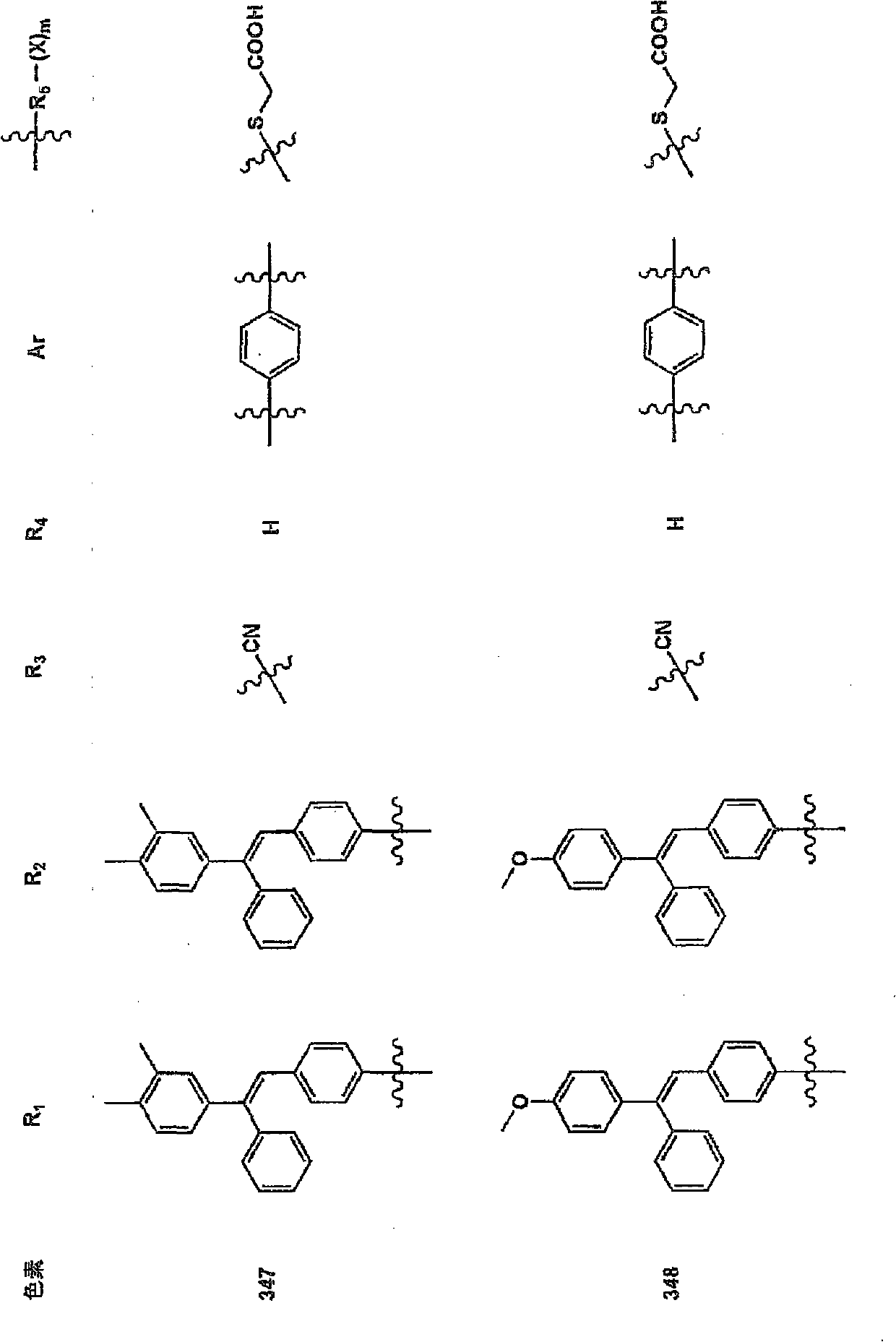
Synthesis Example 2 (Synthesis of Pigment 32)
The dye 32 was synthesized according to the following reaction scheme.
3 equivalents of phosphorus oxychloride was dropped into DMF, and after stirring at room temperature for 30 minutes, DMF of p-methoxytriphenylamine was dropped at 0° C., and the mixture was stirred at room temperature for 3 hours. Cold water was added to the reaction solution, stirred at room temperature for 1 hour, extracted with ethyl acetate, washed with water, dried with magnesium sulfate, concentrated and dried with a rotary evaporator, and treated with a silica column to obtain compound E .
The DMF solution of compound E and 1.05 equivalent of diethylphenyl (p-tolyl) methyl phosphonate was cooled to 0°C, 1.1 equivalent of sodium methoxide was added, and the mixture was stirred for 3 hours. After adding a 0.1 mol/l hydrochloric acid aqueous solution to the reaction solution, it was extracted with ethyl acetate, washed with water, dried with magnesium sulfate, concentrated to dryness with a rotary evaporator, and treated with a silica column to obtain compound F.
The acetic acid solution containing compound F, 1.2 equivalents of thiohydantoin, and 3 equivalents of ammonium acetate was stirred at 120°C for 1 hour. After adding water to the reaction solution, it was extracted with ethyl acetate, washed with water, dried with magnesium sulfate, concentrated to dryness with a rotary evaporator, and treated with a silica column to obtain compound G.
1.1 equivalents of bromoacetic acid and 3 equivalents of potassium hydroxide were added to the ethanol solution of compound G, and the mixture was stirred at 70°C for 1 hour. After concentrating and drying with a rotary evaporator, water and ethyl acetate were added, and the organic layer was removed with a separatory funnel. An excess of 1mol/l hydrochloric acid was added to the water layer, stirred for 5 minutes, extracted with ethyl acetate, washed with water, dried with magnesium sulfate, concentrated to dryness with a rotary evaporator, and treated with a silica column to obtain Pigment 32.
For pigment 32, the structure was confirmed by nuclear magnetic resonance spectroscopy and mass spectrometry.
Compound E
Compound F
Compound F
Other compounds can be synthesized in the same way.
By supporting the dye of the present invention thus obtained on a semiconductor for sensitization, the effects described in the present invention can be produced. Among them, the term “supporting the dye on the semiconductor” includes various forms such as adsorption on the surface of the semiconductor, and when the semiconductor has a porous structure such as a porous structure, the above-mentioned dye is filled into the porous structure of the semiconductor.
In addition, every 1m 2 The total supported amount of the dye of the present invention in the semiconductor layer (which may be a semiconductor) is preferably in the range of 0.01 to 100 mmol, more preferably in the range of 0.1 to 50 mmol, and particularly preferably in the range of 0.5 to 20 mmol.
When the dye of the present invention is used for sensitization treatment, the dye may be used alone, or in combination of multiple types, or combined with other compounds (for example, US Patent No. 4,684,537, US Patent No. 4,927,721, US Patent No. 5,084,365 No. 5,350,644, No. 5,463,057, No. 5,525,440, No. 7-249790, No. 2000-150007, etc.) are used in combination.
When the photoelectric conversion element of the present invention is used as a solar cell described later, in order to broaden the wavelength range of photoelectric conversion as much as possible and effectively use sunlight, it is particularly preferable to use a mixture of two or more dyes having different absorption wavelengths.
When the above-mentioned organic base is a liquid or as a solid, a solution dissolved in an organic solvent is prepared, and the semiconductor of the present invention is immersed in a liquid amine or an amine solution to perform surface treatment.
When a plurality of dyes of the present invention are used in combination, or other dyes are used in combination for sensitization treatment, a mixed solution of each dye may be prepared and used, or separate solutions may be prepared for each dye and immersed in each solution in order. When each solution is prepared for each dye and immersed in each solution in order, the order in which the semiconductor contains the dye or the like may be any order, and the effects described in the present invention can be obtained. In addition, it can be produced by mixing fine particles of semiconductors that have adsorbed the above-mentioned dye alone.
In addition, the details of the sensitization treatment of the semiconductor of the present invention will be specifically described in the part of the photoelectric conversion element described later.
Furthermore, in the case of a semiconductor with a high porosity, it is preferable to complete the adsorption treatment of the dye or the like before water is adsorbed on the semiconductor thin film and the voids inside the semiconductor thin film due to moisture, water vapor, etc. in the voids.
The photoelectric conversion element of the present invention will be described below.
[Photoelectric conversion element]
The photoelectric conversion element of the present invention has at least a semiconductor layer in which the dye of the present invention is supported on a semiconductor, a charge transport layer, and a counter electrode on a conductive support. The semiconductor, the charge transport layer, and the counter electrode will be described in order below.
"semiconductor"
As the semiconductor used in the semiconductor electrode, a simple substance such as silicon and germanium, a compound having elements from groups 3 to 5, and 13 to 15 of the periodic table (also called the periodic table) can be used. Metal chalcogenides (such as oxides, sulfides, selenides, etc.), metal nitrides, and the like.
Preferred metal chalcogenides include oxides of titanium, tin, zinc, iron, tungsten, zirconium, hafnium, strontium, indium, cerium, ytterbium, lanthanum, vanadium, niobium or tantalum, cadmium, zinc, lead, Silver, antimony or bismuth sulfide, cadmium or lead selenide, cadmium telluride, etc. Examples of other compound semiconductors include phosphides of zinc, gallium, indium, and cadmium, selenides of gallium-arsenic or copper-indium, sulfides of copper-indium, and nitrides of titanium.
As a specific example, TiO 2 , SnO 2 , Fe 2 O 3 , WO 3 , ZnO, Nb 2 O 5 , CdS, ZnS, PbS, Bi 2 S 3 , CdSe, CdTe, GaP, InP, GaAs, CuInS 2 , CuInSe 2 , Ti 3 N 4 Etc., preferably TiO 2 , ZnO, SnO 2 , Fe 2 O 3 , WO 3 , Nb 2 O 5 , CdS, PbS, preferably TiO 2 Or Nb 2 O 5 Among them, TiO is particularly preferred 2 (Titanium dioxide).
The semiconductor used in the semiconductor layer may be used in combination of the above-mentioned multiple types of semiconductors. For example, several of the above-mentioned metal oxides or metal sulfides can be used in combination, or 20% by mass of titanium nitride (Ti 3 N 4 ) And use. In addition, a zinc oxide/tin oxide composite described in J. Chem. Soc. Chem. Commun., 15 (1999) may also be formed. At this time, when a component other than a metal oxide or metal sulfide is added as a semiconductor, the mass ratio of the additional component to the metal oxide or metal sulfide semiconductor is preferably 30% or less.
In addition, the semiconductor of the present invention can be surface-treated with an organic base. Examples of the above-mentioned organic bases include diarylamine, triarylamine, pyridine, 4-tert-butylpyridine, polyvinylpyridine, quinoline, piperidine, and amidine, among which pyridine, 4-tert-butylpyridine, Polyvinylpyridine.
When the above-mentioned organic base is a liquid or as a solid, a solution dissolved in an organic solvent is prepared, and the semiconductor of the present invention is immersed in a liquid amine or an amine solution to perform surface treatment.
(Conductive support)
The photoelectric conversion element of the present invention and the conductive support used in the solar cell of the present invention may use a conductive material such as a metal plate, and a structure in which a conductive material is provided on a non-conductive material such as a glass plate and a plastic film material. Examples of materials used in the conductive support include metals (such as platinum, gold, silver, copper, aluminum, rhodium, indium) or conductive metal oxides (such as indium-tin composite oxide, tin oxide doped in Products mixed with fluorine), carbon. The thickness of the conductive support is not particularly limited, but is preferably 0.3 to 5 mm.
In addition, the conductive support on the light-receiving side is preferably substantially transparent, and substantially transparent means that the light transmittance is 10% or more, more preferably 50% or more, and most preferably 80% or more. In order to obtain a transparent conductive support, it is preferable to provide a conductive layer made of a conductive metal oxide on the surface of a glass plate or a plastic film. When a transparent conductive support is used, it is preferable that light enters from the support side.
The surface resistance of the conductive support is preferably 50Ω/cm 2 Below, it is more preferably 10Ω/cm 2 the following.
"Production of Semiconductor Layer"
The manufacturing method of the semiconductor layer of the present invention will be described.
When the semiconductor of the semiconductor layer of the present invention is in the form of particles, the semiconductor can be coated or sprayed on a conductive support to produce a semiconductor layer. In addition, when the semiconductor of the present invention is in a film shape and is not held on a conductive support, it is preferable to bond the semiconductor to the conductive support to produce a semiconductor layer.
As a preferable aspect of the semiconductor layer of the present invention, a method in which fine particles of a semiconductor are used on the above-mentioned conductive support is formed by firing.
When the semiconductor of the present invention is produced by firing, the sensitization (adsorption, filling into the porous layer, etc.) treatment of the semiconductor using a dye is preferably performed after firing. It is particularly preferable to perform the adsorption treatment of the compound immediately after firing and before water is adsorbed on the semiconductor.
Hereinafter, a method of forming a semiconductor electrode preferably used in the present invention by firing using semiconductor fine powder will be described in detail.
(Preparation of coating liquid containing fine semiconductor powder)
First, a coating liquid containing semiconductor fine powder is prepared. The primary particle size of the semiconductor fine powder is preferably fine, and the primary particle size is preferably 1 to 5000 nm, more preferably 2 to 50 nm. The coating liquid containing the semiconductor fine powder can be prepared by dispersing the semiconductor fine powder in a solvent. The semiconductor fine powder dispersed in the solvent is dispersed in the form of primary particles. The solvent is not particularly limited as long as it can disperse the semiconductor fine powder.
The above-mentioned solvent includes water, an organic solvent, and a mixed liquid of water and an organic solvent. As the organic solvent, alcohols such as methanol and ethanol, ketones such as methyl ethyl ketone, acetone, and acetylacetone, and hydrocarbons such as hexane and cyclohexane can be used. Surfactants and viscosity modifiers (polyols such as polyethylene glycol, etc.) can be added to the coating liquid as needed. The range of the concentration of the semiconductor fine powder in the solvent is preferably 0.1 to 70% by mass, and more preferably 0.1 to 30% by mass.
(Coating of coating solution containing fine semiconductor powder and firing treatment of the formed semiconductor layer)
The coating solution containing the semiconductor fine powder obtained above is coated or sprayed on a conductive support, dried, etc., and then fired in the air or in an inert gas to form a semiconductor layer (also called Semiconductor film).
The coating obtained by applying a coating liquid containing semiconductor fine powder to a conductive support and drying is composed of an aggregate of semiconductor fine particles whose particle size corresponds to the primary particle size of the semiconductor fine powder used.
The semiconductor fine particle layer formed on the conductive layer of the conductive support and the like is weak in mechanical strength due to the weak binding force to the conductive support and the mutual binding force of the particles. Therefore, in order to improve the mechanical strength, the formation is firmly fixed to the substrate The semiconductor layer is subjected to the firing treatment of the semiconductor particle layer.
In the present invention, the semiconductor layer may have any structure, but is preferably a porous structure (having voids, also referred to as a porous layer).
Among them, the porosity of the semiconductor layer of the present invention is preferably 10% by volume or less, more preferably 8% by volume or less, and particularly preferably 0.01 to 5% by volume. In addition, the porosity of the semiconductor layer means a porosity having penetration in the thickness direction of the dielectric material, and it is measured using a commercially available device such as a mercury porosimeter (Shimadzu Perase-9220).
The thickness of the semiconductor layer that becomes the fired product film having a porous structure is preferably at least 10 nm or more, and more preferably 500 to 30,000 nm.
During the firing treatment, the actual surface area of the fired film is appropriately adjusted. From the viewpoint of obtaining a fired film having the above porosity, the firing temperature is preferably lower than 1000°C, more preferably in the range of 200 to 800°C, and particularly preferably The range of 300~800℃.
In addition, the ratio of the actual surface area to the apparent surface area can be controlled by the particle size and specific surface area of the semiconductor particles, the firing temperature, and the like. In addition, after the heat treatment, in order to increase the surface area of the semiconductor particles, or to increase the purity of the vicinity of the semiconductor particles, and to increase the efficiency of electron injection from the dye to the semiconductor particles, for example, electroless plating using an aqueous solution of titanium tetrachloride or use The electrochemical plating treatment of titanium trichloride aqueous solution is described.
(Intensification of semiconductors)
The sensitization treatment of the semiconductor is performed by dissolving the dye of the present invention in an appropriate solvent as described above, and immersing the substrate on which the semiconductor is fired in the solution. At this time, it is preferable that the substrate on which the semiconductor layer (also referred to as a semiconductor film) is formed by firing is subjected to a pressure reduction treatment or a heat treatment in advance to remove bubbles in the film. Through such treatment, the dye of the present invention can penetrate deep into the semiconductor layer (semiconductor film), and it is particularly preferred when the semiconductor layer (semiconductor film) is a porous structure film.
The solvent used to dissolve the dye of the present invention is not particularly limited as long as it can dissolve the above-mentioned compound, and does not dissolve or react with the semiconductor. However, in order to prevent moisture and gas dissolved in the solvent from entering the semiconductor film and hindering the sensitization treatment such as adsorption of the above-mentioned compound, it is preferable to perform degassing and distillation purification in advance.
In the dissolution of the above compounds, the preferred solvents used are nitrile solvents such as acetonitrile, alcohol solvents such as methanol, ethanol, and n-propanol, ketone solvents such as acetone and methyl ethyl ketone, diethyl ether, diisopropyl ether, tetrahydrofuran, 1, Ether solvents such as 4-dioxane and halogenated hydrocarbon solvents such as dichloromethane and 1,1,2-trichloroethane can be mixed with multiple solvents. Particularly preferred are acetonitrile, acetonitrile/methanol mixed solvent, methanol, ethanol, acetone, methyl ethyl ketone, tetrahydrofuran, and methylene chloride.
(Temperature and time of sensitization treatment)
The time for immersing the fired semiconductor substrate in the solution containing the dye of the present invention is preferably to penetrate deeply into the semiconductor layer (semiconductor film) to sufficiently perform adsorption, etc., to sufficiently sensitize the semiconductor. In addition, from the viewpoint of inhibiting the degradation of the pigment in the solution from inhibiting the adsorption of the pigment by the decomposition product, it is preferably 3 to 48 hours, and more preferably 4 to 24 hours under 250°C. This effect is particularly remarkable when the semiconductor film is a porous structure film. However, the immersion time is a value at 25°C, and it is not limited to the above when the temperature condition is changed.
The solution containing the pigment of the present invention during immersion can be used by heating it to a temperature that does not boil as long as the pigment does not decompose. The preferred temperature range is 5 to 100°C, more preferably 25 to 80°C, but it is not limited to this when the solvent boils in the above temperature range as described above.
[Photoelectric conversion element]
In addition, the details of the sensitization treatment of the semiconductor of the present invention will be specifically described in the part of the photoelectric conversion element described later.
The charge transport layer is a layer that has a function of rapidly reducing the oxidizer of the dye and transporting holes injected at the interface with the dye to the counter electrode.
The charge transport layer of the present invention is composed of a dispersion of a redox electrolyte and a p-type compound semiconductor (charge transport agent) as a hole transport material as main components.
As the redox electrolyte, I - /I 3 - Department, Br - /Br 3 - Series, quinone/hydroquinone series, etc. Such redox electrolytes can be obtained by conventionally known methods, for example, I - /I 3 - The electrolyte of the system can be obtained by mixing an ammonium salt of iodine and iodine. When these dispersions are in solution, they are called liquid electrolytes, when they are dispersed in a solid polymer at room temperature, they are called solid polymer electrolytes, and when they are dispersed in gel-like substances, they are called gel electrolytes. When a liquid electrolyte is used as the charge transport layer, an electrochemically inert substance is used as the solvent, for example, acetonitrile, propylene carbonate, ethylene carbonate, etc. are used. Examples of solid polymer electrolytes include electrolytes described in JP 2001-160427 A, and examples of gel electrolytes include electrolytes described in "Surface Science" Vol. 21, No. 5, pages 288-293.
As the charge transport agent, it is preferable to have a large band gap in order not to hinder pigment absorption. The band gap of the charge transport agent used in the present invention is preferably 2 eV or more, more preferably 2.5 eV or more. In addition, in order to reduce the dye holes, the ionization potential of the charge transport agent must be lower than the ionization potential of the dye adsorption electrode. The preferable range of the ionization potential of the charge transport agent used in the charge transport layer varies depending on the dye used, but it is generally preferably 4.5 eV to 5.5 eV, and more preferably 4.7 eV to 5.3 eV.
As the charge transport agent, an aromatic amine derivative excellent in hole transport ability is preferred. Therefore, by constituting the charge transport layer mainly with an aromatic amine derivative, the photoelectric conversion efficiency can be further improved. As the aromatic amine derivative, a triphenyldiamine derivative is particularly preferably used. Triphenyldiamine derivatives are particularly excellent in hole transport ability in aromatic amine derivatives. In addition, any of monomers, oligomers, prepolymers, and polymers may be used for such aromatic amine derivatives, or they may be mixed and used. In addition, monomers, oligomers, and prepolymers have low molecular weights and therefore have high solubility in solvents such as organic solvents. Therefore, when the charge transport layer is formed by the coating method, there is an advantage that the charge transport layer material can be prepared more easily. Among them, as the oligomer, a dimer or trimer is preferably used.
As specific aromatic tertiary amine compounds, N,N,N',N'-tetraphenyl-4,4'-diaminophenyl; N,N'-diphenyl-N,N'-bis (3-Methylphenyl)-[1,1'-biphenyl]-4,4'-diamine (TPD); 2,2-bis(4-di-p-tolylaminophenyl)propane; 1 , 1-bis(4-di-p-tolylaminophenyl) cyclohexane; N,N,N',N'-tetra-p-tolyl-4,4'-diaminobiphenyl; 1,1- Bis(4-Di-p-tolylaminophenyl)-4-phenylcyclohexane; Bis(4-dimethylamino-2-methylphenyl)phenylmethane; Bis(4-Di-p-toluene N,N'-diphenyl-N,N'-bis(4-methoxyphenyl)-4,4'-diaminobiphenyl; N,N,N' , N'-tetraphenyl-4,4'-diaminodiphenyl ether; 4,4'-bis(diphenylamino)tetrabiphenyl; N,N,N-tris(p-tolyl)amine; 4-(Di-p-tolylamino)-4'-[4-(Di-p-tolylamino)styryl]stilbene; 4-N,N-diphenylamino-(2-diphenyl Vinyl) benzene; 3-methoxy-4'-N,N-diphenylamino stilbene; N-phenylcarbazole; and the US Patent No. 5,061,569 described in the specification has two dense Compounds that combine an aromatic ring, for example, 4,4'-bis[N-(1-naphthyl)-N-phenylamino]biphenyl (NPD), as described in JP 4-308688 A The aniline unit is connected to a starburst of 4,4',4"-tris[N-(3-methylphenyl)-N-phenylamino]triphenylamine (MTDATA) and the like.
In addition, it is also possible to use a polymer material in which these materials are introduced into the polymer chain or these materials are used as the main chain of the polymer.
Examples of charge transport agents other than aromatic amine derivatives include thiophene derivatives, pyrrole derivatives, and stilbene derivatives.
Specific examples of the charge transport agent are shown below, but the present invention is not limited to these.
[Solar battery]
In addition, the details of the sensitization treatment of the semiconductor of the present invention will be specifically described in the part of the photoelectric conversion element described later.
As long as the counter electrode has conductivity, any conductive material can be used, and it is preferable to use a conductive material having a catalytic ability that enables oxidation of I3-ions and the like, and reduction reactions of other redox ions to proceed at a sufficient rate. . Examples of such conductive materials include platinum electrodes, products in which platinum plating or platinum vapor deposition is performed on the surface of conductive materials, rhodium metal, ruthenium metal, ruthenium oxide, carbon, and the like.
[Solar battery]
The solar cell of the present invention will be described.
As one aspect of the photoelectric conversion element of the present invention, the solar cell of the present invention has a structure that performs optimal design and circuit design for sunlight and performs optimal photoelectric conversion when sunlight is used as a light source. That is, a structure capable of irradiating sunlight to the dye-sensitized semiconductor is formed. When constituting the solar cell of the present invention, it is preferable to house the above-mentioned semiconductor electrode, the charge transport layer, and the counter electrode in a case and seal it, or to seal all of them with a resin.
When the solar cell of the present invention is irradiated with sunlight or an electromagnetic wave equivalent to sunlight, the dye of the present invention carried by the semiconductor absorbs the irradiated light or electromagnetic wave and is excited. The electrons generated by the excitation move to the semiconductor, and then move to the counter electrode via the conductive support, reducing the redox electrolyte of the charge transport layer. On the other hand, the dye of the present invention that transfers electrons to the semiconductor becomes an oxidizer, and is reduced by supplying electrons from the counter electrode through the redox electrolyte of the charge transport layer to return to its original state. At the same time, the redox of the charge transport layer The electrolyte is oxidized and returns to a state where it can be reduced again by electrons supplied from the counter electrode. The flow of electrons in this way can constitute a solar cell using the photoelectric conversion element of the present invention.
Example Embodiment
Example
Hereinafter, the present invention will be described through examples, but the present invention is not limited to these examples.
Example
[Production of photoelectric conversion element 1]
Using screen printing method (coating area 5×5mm 2 ) A titanium dioxide paste (anatase type, primary average particle size (average under microscope observation) 18 nm, polyethylene glycol dispersion) was applied to a fluorine-doped tin oxide (FTO) conductive glass substrate. Coating and drying were repeated 3 times (120°C for 3 minutes), firing at 200°C for 10 minutes and 500°C for 15 minutes to obtain a 15 μm thick titanium dioxide thin film. The same method was used to coat and fire titanium dioxide paste (anatase type, primary average particle size (average under microscope) 400nm, polyethylene glycol dispersion) on the film to form a titanium dioxide film with a thickness of 5 μm.
Dissolve the pigment 1 of the present invention in a mixed solvent of acetonitrile: tert-butanol = 1:1 to prepare 5×10 -4 mol/l solution. The FTO glass substrate coated and sintered with the above-mentioned titanium dioxide was immersed in the solution at room temperature for 3 hours, and the dye was adsorbed to form a semiconductor electrode.
The charge transport layer (electrolyte) contains 0.6mol/l of 1-methyl-3-butylimidazolium iodide, 0.1mol/l of guanidine thiocyanate, 0.05mol/l of iodine, and 4-(tert-butyl)pyridine 0.5mol/l acetonitrile:valeronitrile=85:15 solution. A glass plate on which platinum and chromium were vapor-deposited was used for the counter electrode, and the photoelectric conversion element 1 was fabricated by assembling the previously fabricated semiconductor electrode and charge transport layer with a clamping element.
[Production of photoelectric conversion element 39]
In the production of the photoelectric conversion element 1, the photoelectric conversion elements 2 to 38 were produced in the same manner except that the dye 1 was changed to the dye described in Table 1.
[Production of photoelectric conversion element 39]
In the production of photoelectric conversion element 1, instead of 5×10, which is made by dissolving pigment 1 in a mixed solvent of acetonitrile:tert-butanol=1:1 -4 The mol/l solution becomes the following mixed pigment solution, that is, a 5×10 mixture of pigment 1 dissolved in a mixed solvent of acetonitrile:tert-butanol=1:1 at a ratio of 1:1 -4 mol/l solution and 5×10 of pigment 757 dissolved in a mixed solvent of acetonitrile:tert-butanol=1:1 -4 The photoelectric conversion element 39 was produced in the same manner as the mixed dye solution prepared by the mol/l solution.
Pigment 757
[Production of photoelectric conversion element 40]
In the production of photoelectric conversion element 1, instead of 5×10, which is made by dissolving pigment 1 in a mixed solvent of acetonitrile:tert-butanol=1:1 -4 The mol/l solution becomes the following mixed pigment solution, that is, a 5×10 mixture of pigment 65 dissolved in a mixed solvent of acetonitrile:tert-butanol=1:1 at a ratio of 1:1 -4 mol/l solution and 5×10 of pigment 76 dissolved in a mixed solvent of acetonitrile:tert-butanol=1:1 -4 The photoelectric conversion element 40 was produced in the same manner as the dye solution prepared by the mol/l solution.
[Production of photoelectric conversion element 41]
In the production of photoelectric conversion element 1, dye 1 was changed to dye 801, and the charge transport layer (electrolyte) contained 0.6 mol/l of 1-methyl-3-butylimidazolium iodide and 0.1 mol/l of lithium iodide. 1. A solution of 3-methoxypropionitrile containing 0.05 mol/l of iodine and 0.5 mol/l of 4-(tert-butyl)pyridine, and other than that, the photoelectric conversion element 41 was produced in the same manner.
[Production of photoelectric conversion element 44]
In the production of the photoelectric conversion element 41, the photoelectric conversion element 42 was produced in the same manner except that the dye 801 was changed to the dye 802.
[Production of photoelectric conversion element 43]
Using screen printing method (coating area 5×5mm 2 ) Apply titanium dioxide paste (anatase type, primary average particle size (average under microscope) 18nm, polyethylene glycol dispersion) to a fluorine-doped tin oxide (FTO) conductive glass substrate, and perform 10 It was fired in minutes and fired at 450°C for 15 minutes to obtain a titanium dioxide thin film with a thickness of 1.5 μm.
Dissolve the pigment 5 of the present invention in a mixed solvent of acetonitrile: tert-butanol = 1:1 to prepare 5×10 -4 mol/l solution. The FTO glass substrate coated and sintered with the above-mentioned titanium dioxide was immersed in the solution at room temperature for 3 hours, and the dye was adsorbed to form a semiconductor electrode.
Next, dissolve in a mixed solution of chlorobenzene:acetonitrile=19:1 so that the aromatic amine derivative 2,2',7,7'-tetra(N,N'-bis(4- Methoxyphenyl) amine-9,9'-Spiro-OMeTAD (Spiro-OMeTAD) is 0.17mol/l, so that N(PhBr) as a hole dopant 3 SbCl 6 Is 0.33mmol/l, so that Li[(CF 3 SO 2 ) 2 N] was 15 mmol/l and tert-butylpyridine was 50 mmol/l to prepare a coating liquid for forming a hole layer. Then, the coating solution for forming a hole layer is applied to the upper surface of the semiconductor layer to which the above-mentioned photosensitizing dye is adsorbed and bound by a spin coating method to form a charge transport layer. Furthermore, 90 nm gold was vapor-deposited by a vacuum vapor deposition method to produce a counter electrode, and a photoelectric conversion element 43 was produced. In the above-mentioned coating by the spin coating method, the rotation speed of the spin coating was set to 1000 rpm.
[Production of photoelectric conversion element 44]
The photoelectric conversion element 44 was produced in the same manner as the photoelectric conversion element 43 except that the dye of the photoelectric conversion element was changed to 801.
[Evaluation of photoelectric conversion element]
By using a solar simulator (Ehiro Seiki), the produced photoelectric conversion element is irradiated with 100mW/cm from a xenon lamp that has passed an AM filter (AM-1.5) 2 Quasi-sunlight. That is, for the photoelectric conversion element, the current-voltage characteristics are measured at room temperature using an IV tester, the short-circuit current density (Jsc), the open voltage (Voc), and the shape factor (FF) are obtained, and the photoelectric conversion efficiency (η (%)).
Table 1 shows the results of the evaluation.
[Table 1]
Photoelectric conversion element No. Pigment Open voltage (mV) Short-circuit current density (mA/cm 2 ) Photoelectric conversion efficiency (%) Remarks 1 1 720 14.4 6.6 Invention 2 3 710 14.6 6.9 Invention 3 5 750 16.1 8.7 Invention 4 8 760 12.6 5.5 Invention 5 12 690 13.8 6.3 Invention 6 21 730 14.1 6.6 Invention 7 22 660 11.3 4.9 Invention 8 32 700 14.9 7.0 Invention 9 54 700 12.1 6.1 Invention
Photoelectric conversion element No. Pigment Open voltage (mV) Short-circuit current density (mA/cm 2 ) Photoelectric conversion efficiency (%) Remarks 10 57 670 11.9 5.1 Invention 11 76 690 13.5 5.9 Invention 12 95 690 13.3 5.9 Invention 13 128 670 10.5 4.9 Invention 14 171 740 10.1 4.5 Invention 15 193 700 9.5 4.0 Invention 16 223 700 13.3 6.0 Invention 17 245 740 10.8 5.3 Invention 18 278 670 9.9 4.1 Invention 19 316 710 12.9 6.0 Invention 20 407 660 14.6 6.4 Invention 21 409 630 12.1 4.6 Invention 22 418 700 14.2 6.5 Invention 23 447 650 8.9 3.9 The invention 24 510 670 7.9 3.8 The invention 25 550 650 7.8 3.7 The invention 26 609 690 13.2 6.2 The invention 27 630 670 8.7 3.8 The invention 28 637 740 14.1 7.6 The invention 29 638 720 13.2 7.1 The invention 30 649 730 13.3 7.3 The invention
Photoelectric conversion element No. Pigment Open voltage (mV) Short-circuit current density (mA/cm 2 ) Photoelectric conversion efficiency (%) Remarks 31 661 740 13.8 7.4 The present invention 32 673 700 13.2 6.9 The present invention 33 685 690 14.3 6.9 The present invention 34 701 670 9.0 4.3 The present invention 35 715 680 11.1 5.1 The present invention 36 721 680 11.3 5.1 The present invention 37 733 670 11.8 5.2 The present invention 38 745 660 9.9 4.3 The present invention 39 1/757 740 14.8 6.6 The present invention 40 65/76 710 13.7 6.0 The present invention 41 801 670 7.9 3.1 Comparative example 42 802 660 7.2 2.8 Comparative example 43 5 830 9.1 3.8 The present invention 44 801 660 4.2 0.9 Comparative example
From Table 1, it can be seen that the photoelectric conversion element 13 using the dye having an imidazolinone skeleton of the present invention has short-circuit current density and conversion efficiency compared with the photoelectric conversion element 41 using a comparative dye having a rhodanine skeleton. improve. In addition, the photoelectric conversion elements 39 and 40 using a plurality of dyes have also found improvements in conversion efficiency. Compared with the photoelectric conversion element 44, the photoelectric conversion element 43 has improved short-circuit current density, open voltage, and conversion efficiency. In the photoelectric conversion elements 1 to 38 using the dye having an imidazolinone skeleton of the present invention, the conversion efficiency was also improved. In addition, some of the pigments of the present invention develop aggregation due to intermolecular interactions, the absorption wavelength shifts to long wavelengths, or the amount of adsorbed pigments increases, and therefore absorbs more wavelengths of light, which is considered to be a factor in the improvement of conversion efficiency.
According to the present invention, it is possible to provide a photoelectric conversion element and a solar cell using a compound (dye) that is novel and has good adsorption properties for oxide semiconductors and high photoelectric conversion efficiency.
PUM
Property | Measurement | Unit |
Surface resistance | <= 50.0 | Ω/cm² |
Description & Claims & Application Information
We can also present the details of the Description, Claims and Application information to help users get a comprehensive understanding of the technical details of the patent, such as background art, summary of invention, brief description of drawings, description of embodiments, and other original content. On the other hand, users can also determine the specific scope of protection of the technology through the list of claims; as well as understand the changes in the life cycle of the technology with the presentation of the patent timeline. Login to view more.
Similar technology patents
A nanofiber film blood lead color sensor and detection method thereof
Owner:DONGHUA UNIV
Vehicle seat containing activated carbon
Owner:SUZHOU HUANGZHANGMEIZU IND DESIGN
Preparation method of secondary functionalized double-coating modified polyether sulfone lithium-sulfur battery diaphragm
Owner:CENT SOUTH UNIV
A kind of diatom mud coating that adds amino acid to remove formaldehyde
Owner:天津朗发特环保科技有限公司
Environment-friendly cleaning dust removal adjustable watering cart
Owner:甘肃方舟苑环保装备制造有限公司
Classification and recommendation of technical efficacy words
- Improve photoelectric conversion efficiency
- Good adsorption
Broad-spectrum absorption black silicon solar cell structure and preparation method thereof
Owner:INST OF SEMICONDUCTORS - CHINESE ACAD OF SCI
Method and corrosive liquid for making texture surface of monocrystalline silicon
Owner:JETION SOLAR HLDG
Preparation method of black-edge-free high-efficiency polycrystalline silicon ingot
ActiveCN104328490AImprove photoelectric conversion efficiencyLow efficiency leakage ratio is reduced
Owner:江苏美科太阳能科技股份有限公司
Method and device for manufacturing solar cell electrode
Owner:JIAWEI RENEWABLE ENERGY CO LTD
Nitrous oxides gas adsorbing substance and preparation method thereof
Owner:SHANGHAI NAT ENG RES CENT FORNANOTECH
Coal gasification wastewater treatment method
Owner:ENN SCI & TECH DEV
Sodium bentonite processing agent for blue-green algae and preparation method thereof
Owner:WUHU XIANGRONG FOOD
Flue gas adsorption desulfurizer and preparation method thereof
Owner:WUHU ZHONGLU IND
Preparation method for hyperbranched polycarboxylic acid polymer scale inhibitor
Owner:CHENGDU ORGANIC CHEM CO LTD CHINESE ACAD OF SCI