Unlock instant, AI-driven research and patent intelligence for your innovation.

FPGA-based method for realizing linear frequency-modulated signal

A technology of linear frequency modulation signal and implementation method, applied in the direction of automatic power control, electrical components, etc., can solve the problems of high price, inability to satisfy users, and much poor application flexibility.

Active Publication Date: 2010-10-20
成都市国科微电科技合伙企业(有限合伙)
View PDF0 Cites 19 Cited by
  • Summary
  • Abstract
  • Description
  • Claims
  • Application Information

AI Technical Summary

Problems solved by technology

However, the current dedicated DDS is only suitable for certain requirements and has certain limitations, so it cannot meet various requirements of users.
[0003] With the rapid development of science and technology, major chip manufacturers in the market have successively launched high-performance and multi-functional DDS chips produced by advanced CMOS technology, providing circuit designers with a variety of choices. Common DDS chips include AD9850, AD9851, AD9854, AD9954, etc., but because the chip has solidified its specific functions, it is much less flexible for different applications. For example, if you want to generate AM waves, you must connect an analog multiplier
And for the powerful AD9954, the price is very expensive, especially in some occasions, the special DDS chip has a big gap with the system requirements in terms of control mode and frequency setting rate.
Moreover, there are a variety of direct digital synthesis signal source chips on the market, such as the AD9850 of the American AD company. Due to the high price and fixed single function of this type of special chip, its application is limited.

Method used


Image

  • FPGA-based method for realizing linear frequency-modulated signal
  • FPGA-based method for realizing linear frequency-modulated signal
  • FPGA-based method for realizing linear frequency-modulated signal

Examples


Embodiment Construction

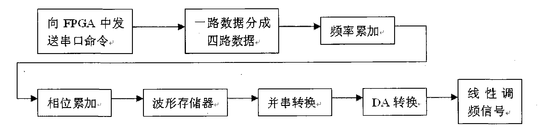
[0026] refer to figure 1 , the chirp signal realization process of the present invention is as follows:

[0027] Step 1. Send a serial port command to the FPGA, and select different working modes that have been set in the FPGA to generate one channel of data.

[0028] Set different working modes, including: center frequency fO is 80M, bandwidth B is 100M, duration Tp is 100us, center frequency fO is 130M, bandwidth B is 100M, duration Tp is 100us, center frequency fO is 80M, bandwidth B is 45M, and the duration Tp is 100us. These working modes quantify the initial frequency f and modulation frequency g according to the center frequency and bandwidth, where f=fO-B / 2, g=B / Tp.

[0029] Step 2. Divide one channel of data into four channels of data through four extractions. Four extractions refer to extracting one channel of data every four data. The first channel is extracted from the first number, and the second channel is extracted from the second The number starts to be extra...


PUM


Abstract

The invention discloses a method for realizing a linear frequency-modulated signal, which mainly solves the problem that the existing method has single function. The method comprises the following steps: sending a serial port command to FPGA, selecting different operating modes which have already been set in FPGA and generating one-way data; dividing the one-way data into four ways; using the four-way data as frequency control words and carrying out frequency accumulation on the frequency control words by an accumulator; using the results of frequency accumulation as the phase control words and carrying out phase accumulation; using the results of phase accumulation as the address of a waveform memory and addressing the amplitudes of sine waves stored in the memory; using an LVDS module in the IP core in FPGA to carry out parallel-serial conversion on the four-way addressing results; and carrying out DA conversion on the results of parallel-serial conversion and finally obtaining the analog waveform of the linear frequency-modulated signal. In the method, the linear frequency-modulated signal with different parameters can be generated, the sampling rate is as high as 960M and the linear frequency-modulated signal can be used as the signal source.

Description

technical field [0001] The invention belongs to the technical field of digital signal processing, in particular to a method for realizing a linear frequency modulation signal by using FPGA, which can be used as a signal source. Background technique [0002] Direct frequency synthesizer is a new frequency synthesis method of digital technology, which is based on the theory of digital signal processing and directly synthesizes the required waveform from the concept of phase. With the development of direct digital frequency synthesis DDS technology, many chip companies have developed their own DDS ASICs, which together with D / A converters and low-pass filters LPF can form arbitrary waveform signal generators. , communications and other fields have a wide range of applications. However, the current dedicated DDS is only suitable for certain requirements and has certain limitations, so it cannot meet various requirements of users. [0003] With the rapid development of science ...

Claims


Application Information

Patent Timeline
IPC IPC(8): H03L7/18
Inventor 王海娟全英汇李亚超邢孟道黄明慧宋猛
Owner 成都市国科微电科技合伙企业(有限合伙)