Interrupt processing method of multi-PCIE (Peripheral Component Interface Express) equipment system

A system interrupt and processing method technology, applied in the direction of electrical digital data processing, instruments, etc., can solve the problem of inability to handle multiple PCIE device interrupts, and achieve the effect of shortening the interrupt delay

Active Publication Date: 2010-10-27
HANGZHOU HIKVISION DIGITAL TECH
View PDF0 Cites 31 Cited by
  • Summary
  • Abstract
  • Description
  • Claims
  • Application Information

AI Technical Summary

Problems solved by technology

[0006] In the process of implementing the present invention, the inventor finds that there are at least the following problems in the prior art: when multiple PCIE devices generate interrupts at the same time, multiple MSI messages will be generated, and after the PCIE main bridge receives multiple MSI messages, multiple MSI messages will be generated. The interrupt vector numbers are sequentially written into the interrupt registers pre-

Method used


Image

  • Interrupt processing method of multi-PCIE (Peripheral Component Interface Express) equipment system
  • Interrupt processing method of multi-PCIE (Peripheral Component Interface Express) equipment system
  • Interrupt processing method of multi-PCIE (Peripheral Component Interface Express) equipment system

Examples


Embodiment 1

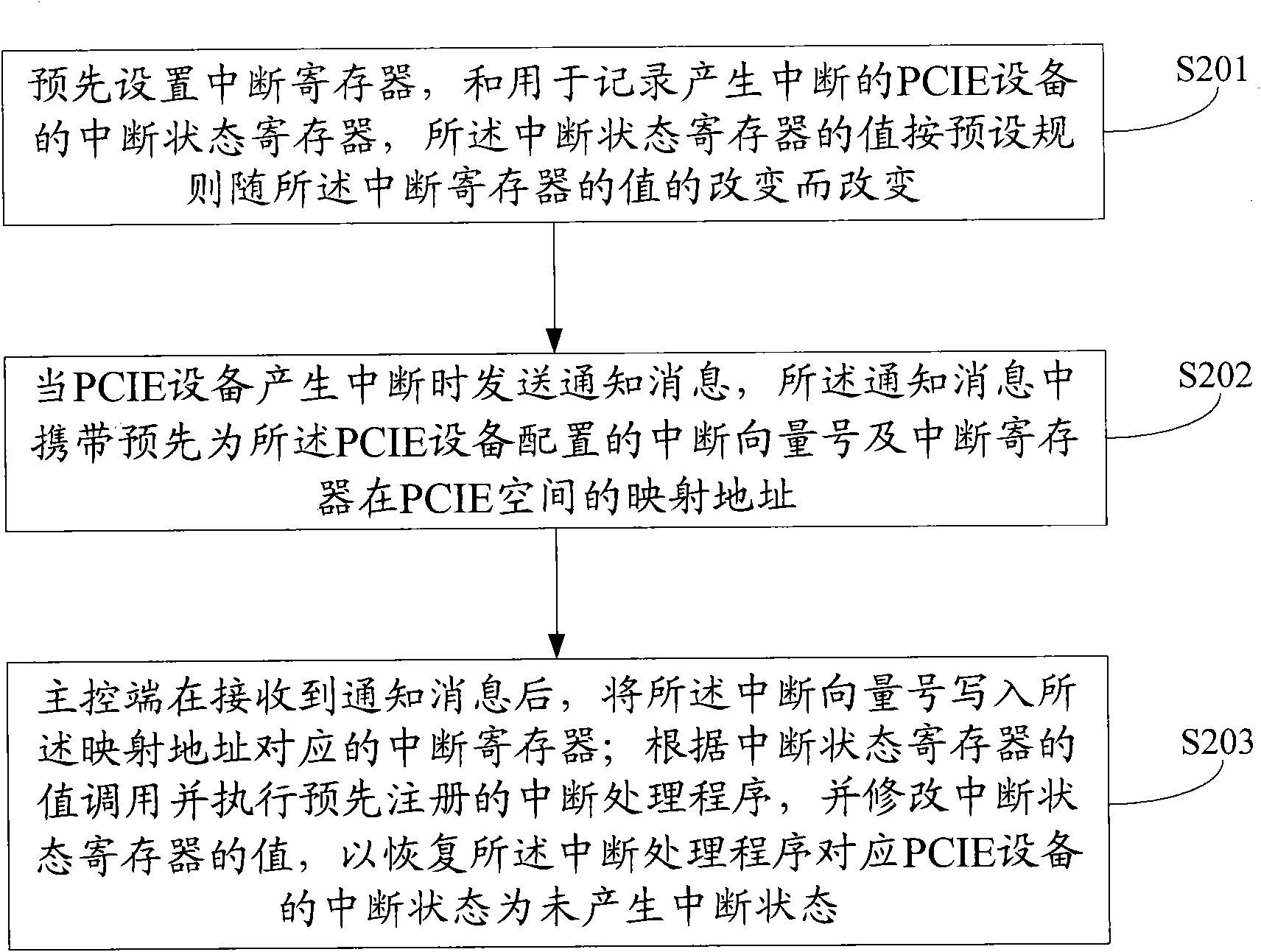
[0050] see figure 2 , the embodiment of the present invention provides a kind of multi-PCIE device system interruption processing method, comprises the following steps:

[0051] Step S201: Presetting an interrupt register and an interrupt status register for recording the interrupted PCIE device, the value of the interrupt status register changes with the value of the interrupt register according to preset rules.

[0052] Step S202: Send a notification message when the PCIE device generates an interrupt, the notification message carrying the interrupt vector number pre-configured for the PCIE device and the mapping address of the interrupt register in the PCIE space.

[0053] Step S203: After receiving the notification message, the master control terminal writes the interrupt vector number into the interrupt register corresponding to the mapping address; calls and executes the pre-registered interrupt handler according to the value of the interrupt status register, and modifi...
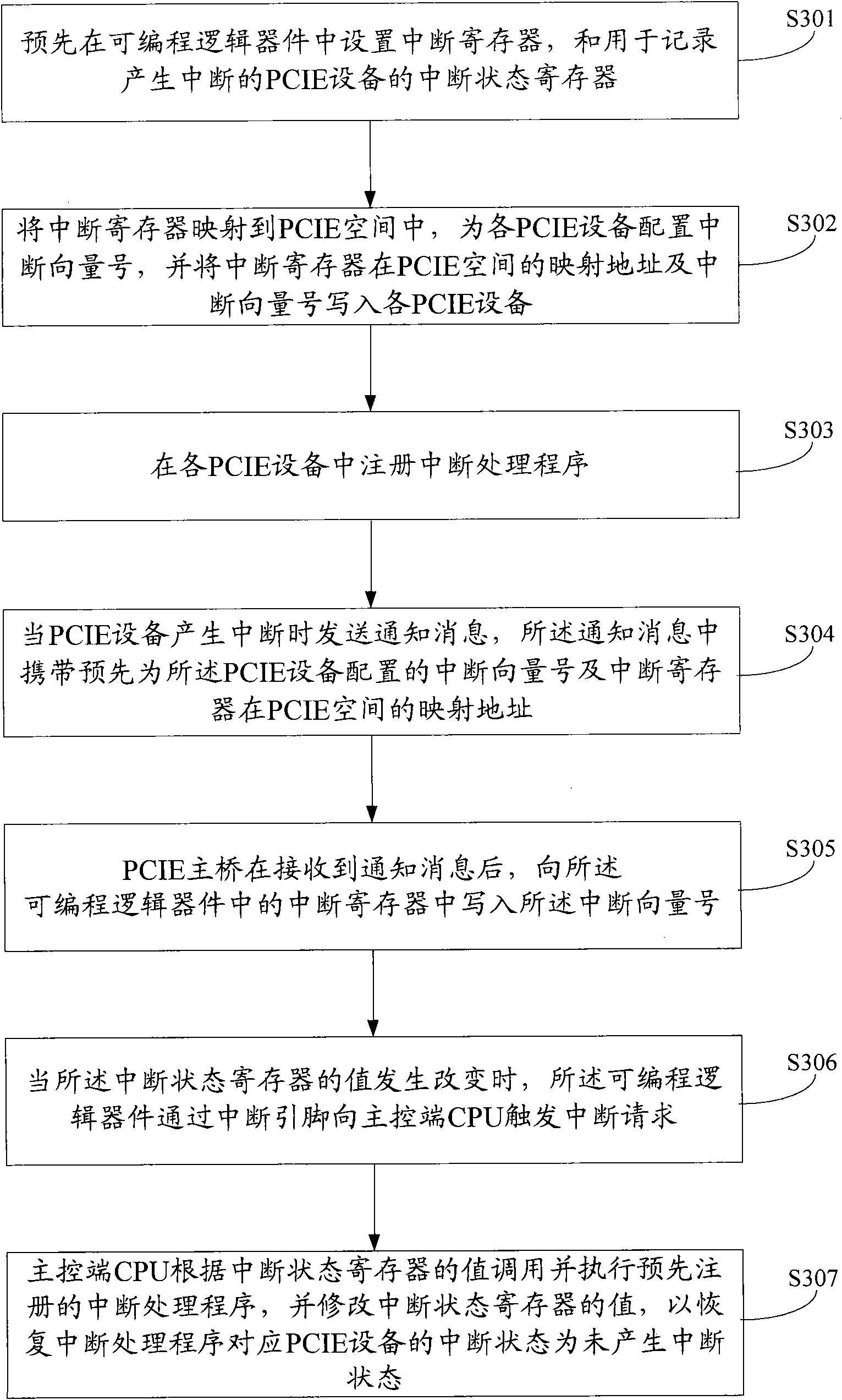
Embodiment 2

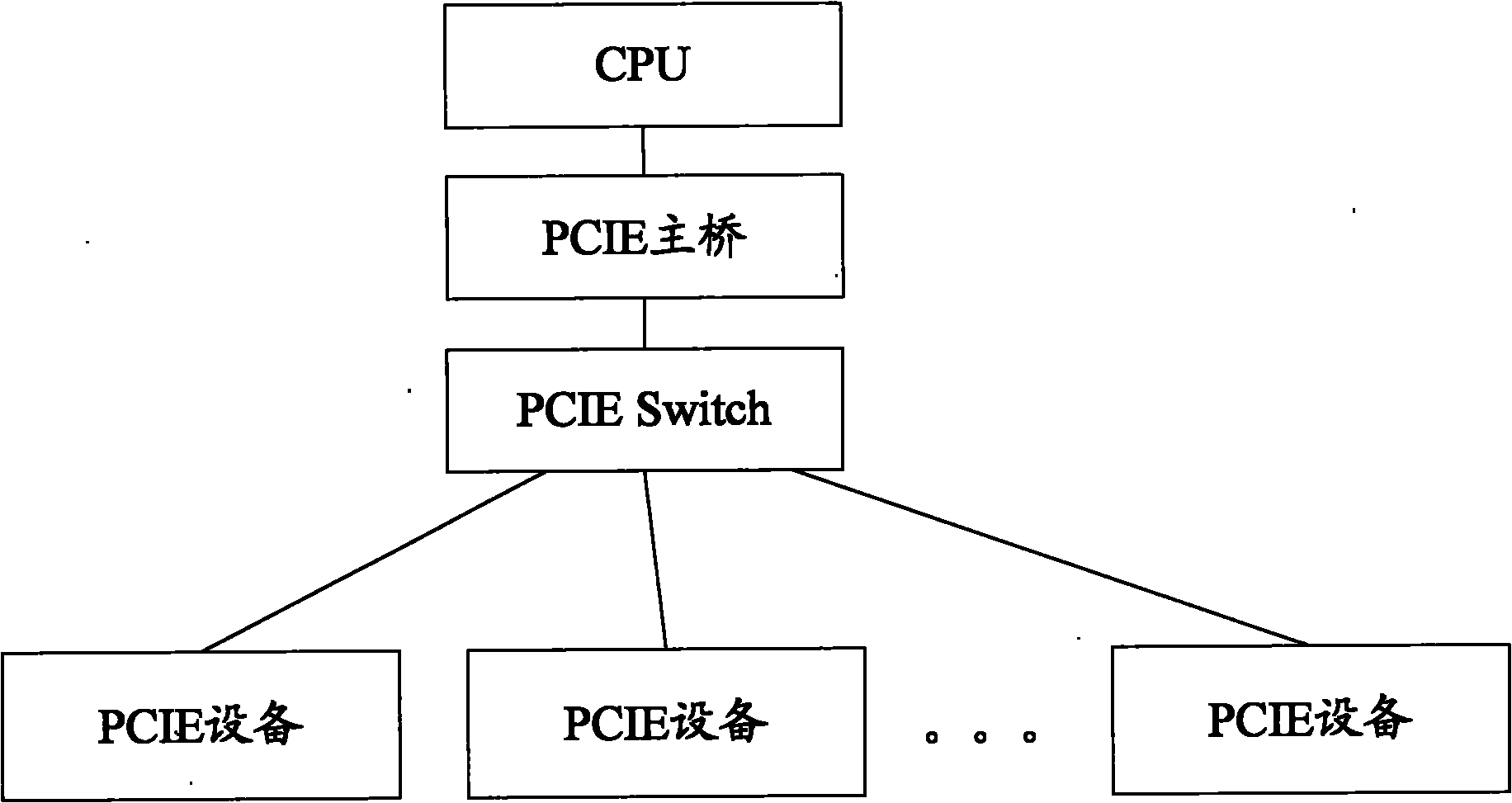
[0057] see image 3 , the embodiment of the present invention provides a preferred multi-PCIE device system interrupt processing method, combined with reference Figure 4 , preferably, the main control end comprises central processing unit CPU401, the PCIE main bridge 402 that links to each other with CPU401, is used for the data conversion between the CPU bus data format supported by CPU401 and the data format supported by each PCIE device, and the possible linking to each other with CPU401 Program logic device 403 . Of course, according to actual application scenarios, a PCIE Switch may also be included between the PCIE main bridge 402 and each PCIE device, for coordinating data exchange among multiple PCIE devices.

[0058] Preferably, the programmable logic device may be CPLD or FPGA or the like.

[0059] In practical applications, the PCIE main bridge 402 can be set on the motherboard, or integrated in the CPU 401 .

[0060] The method provided by the embodiment of the...


PUM


Abstract

The invention discloses an interrupt processing method of a multi-PCIE (Peripheral Component Interface Express) equipment system, relating to the field of automatic control. In the invention, an interrupt register and an interrupt state register are arranged in advance, and the value of the interrupt state register changes along with the variation of a value of the interrupt register based on a preset rule; a notification message is sent when PCIE equipment generates interrupt, and an interrupt vector number and an interrupt register address which are configurated to the PCIE equipment in advance are carried in the message; after receiving the notification message, a main control end writes the interrupt vector number into the interrupt register corresponding to a mapping address; and an interrupt processing program which is registered in advance is called and executed based on the value of the interrupt state register, and the value of the interrupt state register is revised to restore an interrupt state of the PCIE equipment corresponding to the interrupt processing program into a non-interrupt state. The invention can process interrupt simultaneously generated by a plurality of PCIE equipments, and PCIE equipment which does not support an MSI (Medium-scale Integration) interrupt mode can apply the invention, therefore, the interrupt processing efficiency of the system is improved.

Description

technical field [0001] The invention relates to the field of automatic control, in particular to a multi-PCIE device system interrupt processing method. Background technique [0002] PCIE (Personal Computer Expansion Bus Interface) devices are a new generation of new architectures that can provide massive bandwidth and rich features to enable exciting new graphics applications. see figure 1 , which is a schematic diagram of the topology structure of a multi-PCIE device system, including a master control terminal and several PCIE devices as end points (End Point), wherein the master control terminal includes a CPU and a PCIE host bridge (PCIE host bridge), and the PCIE host bridge is mainly used for Realize the data conversion between the CPU bus data format supported by the CPU and the data format supported by each PCIE device. Usually, a PCIE Switch (switch) is also included to coordinate data exchange between multiple PCIE devices. [0003] Currently, in a system with mu...

Claims


Application Information

Patent Timeline
IPC IPC(8): G06F13/24
Inventor 栾焕志赵先林胡扬忠邬伟琪
Owner HANGZHOU HIKVISION DIGITAL TECH
Why Eureka
Try Eureka