
Atomic force microscope probe based on structures of carbon nano tube and planar wave guide

An atomic force microscope and planar waveguide technology, applied in waveguide, waveguide-type devices, scanning probe technology, etc., can solve problems such as large needle tip diameter, lack of high-frequency characteristics, and unsatisfactory mechanical properties

Inactive Publication Date: 2010-11-03
PEKING UNIV
View PDF4 Cites 21 Cited by
  • Summary
  • Abstract
  • Description
  • Claims
  • Application Information

AI Technical Summary

Problems solved by technology

There have been reports on high-frequency probes on AFM (A.Karbassi, C.A.Paulson, Y.Wang, A.Bettermann, and D.W.van der Weide,"Localized Microwave Measurement using AFM-Compatible Scanning Nearfield MicrowaveMicroscope Cantilever with Ultra-tall Coaxial Probe”, 2007IEEE Antennas and Propagation Society International Symposium 3336-9, 2008), but the high-frequency characteristics of the commonly used AFM tip materials (silicon, silicon nitride or metal, etc.) are still lacking, and the tip diameter is large and the mechanical properties are poor not ideal

Method used


Image

  • Atomic force microscope probe based on structures of carbon nano tube and planar wave guide
  • Atomic force microscope probe based on structures of carbon nano tube and planar wave guide
  • Atomic force microscope probe based on structures of carbon nano tube and planar wave guide

Examples


Embodiment Construction

[0016] Embodiments of the present invention are described in more detail below with reference to the accompanying drawings of the present invention.

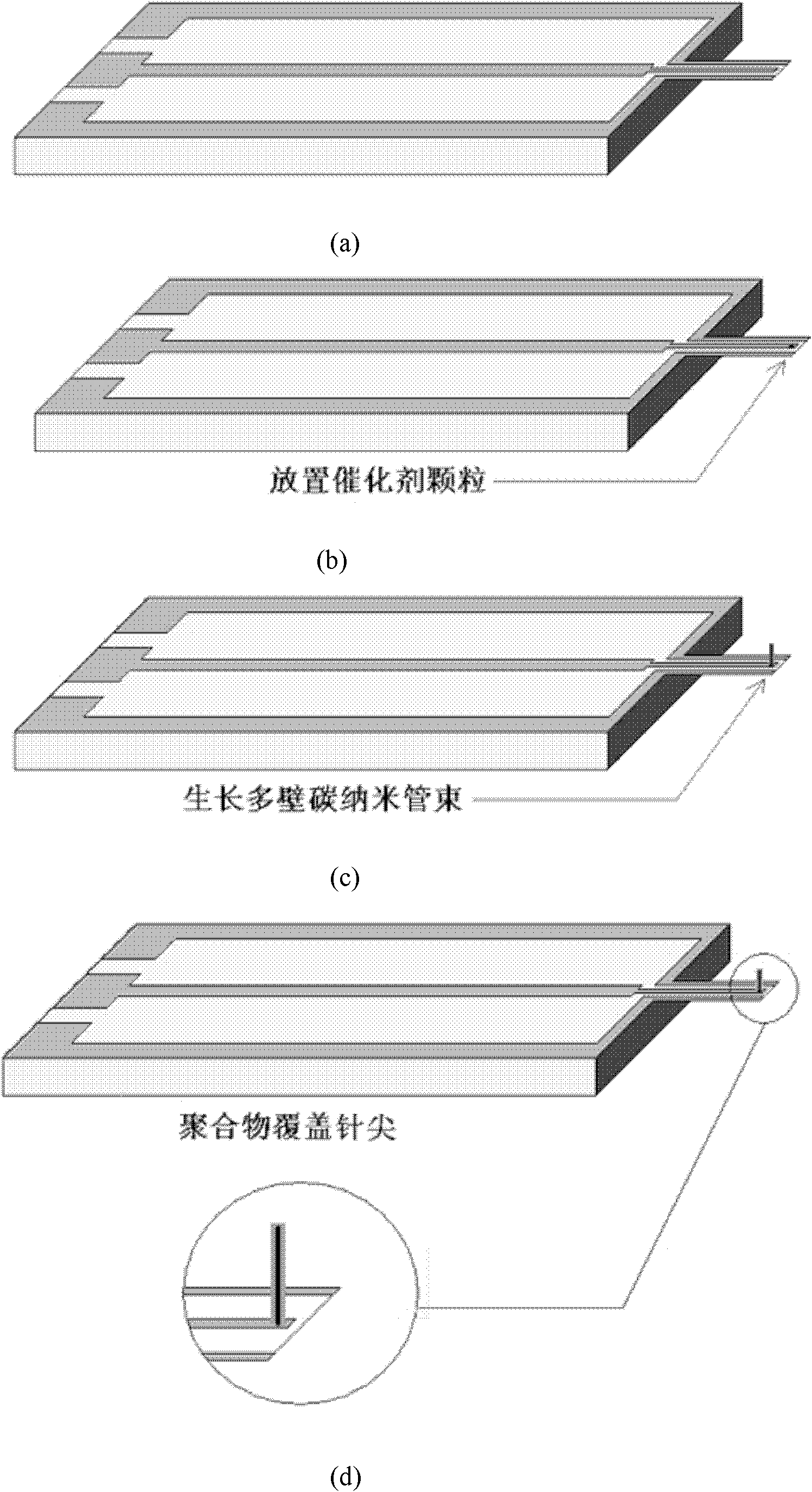
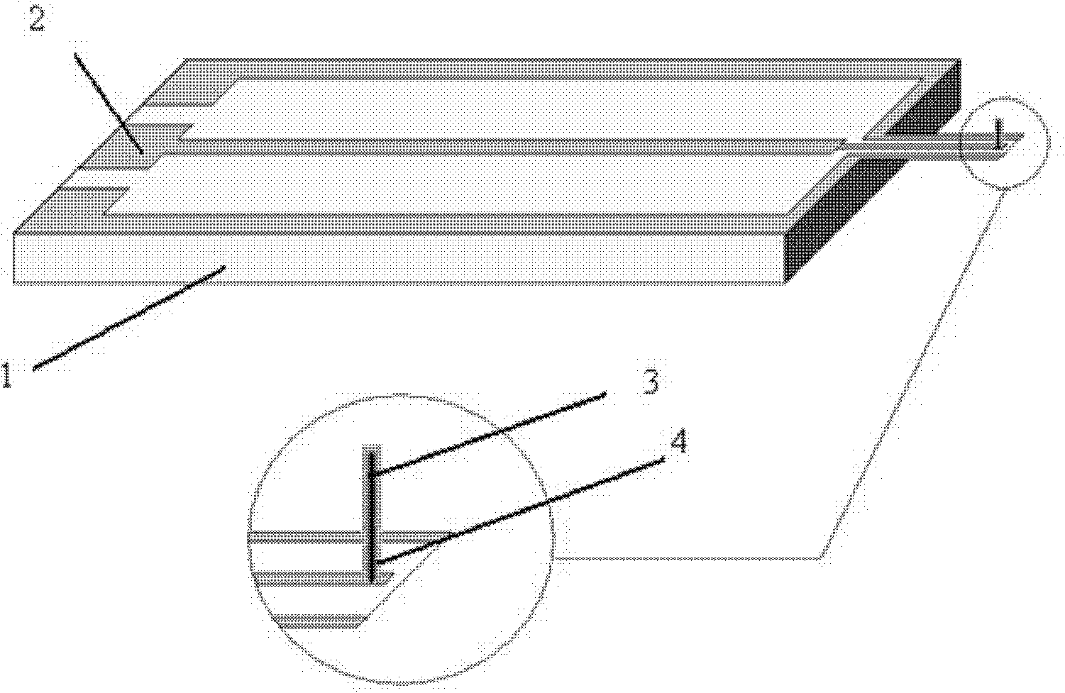
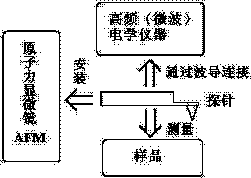
[0017] The invention provides an AFM probe that is relatively easy to prepare and can simultaneously measure surface morphology, high-frequency (to microwave band) electrical properties, etc. of samples such as nanomaterials, devices, and various soft substances. The device can accurately measure the surface topography of a sample by being installed to and operated by the AFM, and simultaneously measure the high-frequency characteristics of the sample in situ. The probe device can, but is not limited to, separately measure surface topography and high-frequency electrical properties. The characteristics of the carbon nanotubes at the needle tip can be controlled, but not limited to, by controlling the growth conditions and subsequent polymer encapsulation treatment. The probe setup allows multiple measurements to be made by chan...


PUM


Abstract

The invention provides an atomic force microscope probe based on structures of a carbon nano tube and a planar wave guide, belonging to the technical field of micronano. The atomic force microscope probe comprises a probe substrate platform compatible with the atomic force microscope, a planar wave guide attached to the surface of the probe substrate platform and a carbon nano tube as a probe point. when in use, the planar waveguide structure is connected to a high-frequency (microwave) measuring instrument, and the whole probe is arranged to the atomic force microscope (AFM) and is scanned or positioned by the standard operation of the AFM, so that the surface topography of a measuring sample can be measured and the high-frequency characteristics of the measuring sample can be synchronously measured in situ. Particularly, the high-frequency (microwave) transmission with small signal loss can be carried out by using the planar waveguide; the carbon nanotube as the probe point has excellent high-frequency transmission property and the mechanical property; the diameter of the carbon nanotube can be adjusted by controlling growth conditions; in addition, the invention is suitable for high-precision and high-frequency (high-frequency) measurement.

Description

technical field [0001] The invention belongs to the field of micro / nano measurement technology, and specifically relates to a planar waveguide structure and a carbon nanotube tip that can be installed in an atomic force microscope (AFM). Measurement of surface morphology, high frequency (to microwave band) electrical properties, etc. Background technique [0002] At the nanoscale, various materials and devices with low-dimensional structures have attracted much attention due to their excellent characteristics and huge potential application value, especially the electrical transport characteristics are the focus of research and application. With the in-depth study of electrical properties, the method of using DC electrical measurement methods to study and characterize nanomaterials and devices is becoming more and more mature, and the relevant physical mechanisms, including various transport models, are becoming clearer. [0003] However, due to the complexity of experiments...

Claims


Application Information

Patent Timeline
Patent Type & Authority Applications(China)
IPC IPC(8): G01Q60/38H01P3/00
Inventor 许胜勇孙伟强
Owner PEKING UNIV
Learn More