Preparation method of trenches of polyimide-embedded syconoid ridge type devices

A technology of polyimide and its production method, which is applied in the field of lithography process for manufacturing semiconductor devices, and can solve problems such as difficult lithography process

Inactive Publication Date: 2010-11-10
INST OF SEMICONDUCTORS - CHINESE ACAD OF SCI
View PDF0 Cites 5 Cited by
  • Summary
  • Abstract
  • Description
  • Claims
  • Application Information

AI Technical Summary

Problems solved by technology

For example, for a ridge waveguide high-frequency laser with a wavelength of 1.5um, it is required to bury polyimide in each 7um channel on both sides of the 1.5um strip-

Method used


Image

  • Preparation method of trenches of polyimide-embedded syconoid ridge type devices
  • Preparation method of trenches of polyimide-embedded syconoid ridge type devices
  • Preparation method of trenches of polyimide-embedded syconoid ridge type devices

Examples


Embodiment example

[0027] Taking a double-groove ridge laser with a wavelength of 1.5um as an example, after implementing the manufacturing method of the polyimide-filled double-groove ridge device channel of the present invention, the operation is as follows:

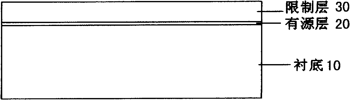
[0028] Step 1: growing an active layer 20 and a confinement layer 30 on the surface of the substrate 10;

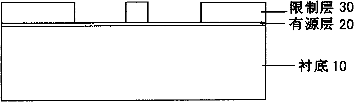
[0029] Step 2: making a photolithography pattern on the surface of the confinement layer 30;

[0030] Step 3: photolithography, etching a double-groove-ridge structure on the surface of the confinement layer 30, and the etching depth reaches the surface of the active layer 20;

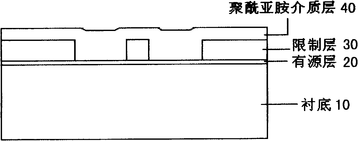
[0031] Step 4: Coat the polyimide dielectric layer 40 in the double-groove ridge structure and the surface of the limiting layer 30 for pre-curing; the pre-curing time is 20-40 minutes, using a desktop electric drying oven, and the curing temperature is 110- 120°C;

[0032] Step 5: Apply photoresist 50 on the surface of polyimide dielectric layer 40, and d...


PUM


Abstract

The invention discloses a preparation method of trenches of polyimide-embedded syconoid ridge type devices, comprising the following steps: step 1: growing a source layer and a limiting layer on the surface of a substrate in sequence, which are used as a basic structure of a device; step 2: manufacturing a photoetching graph on the surface of the limiting layer; step 3: photoetching: etching a syconoid ridge type structure on the surface of the limiting layer, wherein, the etching depth reaches the surface of the source layer; step 4: coating polyimide dielectric layers in the syconoid ridge type structure and on the surface of the limiting layer, and procuring; step 5: coating photoresist on the surface of the polyimide dielectric layer, and drying; and step 6: exposing, developing and removing the polyimide dielectric layers on the syconoid ridge type structure and on the surface of the limiting layer, and curing to finish manufacture of the device.

Description

technical field [0001] The invention belongs to the technical field of photolithography technology for manufacturing semiconductor devices, in particular to a method for manufacturing polyimide-filled double-groove-ridge-type device channels, which can improve the high-frequency performance of the device. By controlling the development rate, this difficult process is completed. Background technique [0002] With the rapid development of optical communication technology, the bandwidth requirements of optoelectronic devices are getting higher and higher. It is not only necessary to optimize the device structure, but also to innovate the dielectric manufacturing process to reduce capacitance. For example, for a ridge waveguide high-frequency laser with a wavelength of 1.5um, it is required to bury polyimide in each 7um channel on both sides of the 1.5um strip-shaped mesa in the active layer, and remove it from other places, especially the top of the 1.5um strip-shaped mesa. T...

Claims


Application Information

Patent Timeline
IPC IPC(8): H01S5/22
Inventor 王宝军朱洪亮赵玲娟王圩潘教青梁松边静安心王伟周代兵
Owner INST OF SEMICONDUCTORS - CHINESE ACAD OF SCI
Why Eureka
Try Eureka