Method of designing integrated circuit and computer system with the method

An integrated circuit and path technology, applied in computer-aided design, computing, electrical digital data processing, etc., can solve problems such as resistance timing problems, and achieve the effect of increasing execution efficiency, saving area and power, and reducing design cycle time.

Active Publication Date: 2013-03-13
TAIWAN SEMICON MFG CO LTD
View PDF3 Cites 0 Cited by
  • Summary
  • Abstract
  • Description
  • Claims
  • Application Information

AI Technical Summary

Problems solved by technology

However, using fixed metal element widths for some paths will cause timing issues
For example, if the critical dimension (CD) of a metal element is too small, the resistor (R) can cause timing problems
On the other hand, if the critical dimension of a metal component is too large, the capacitance (C) will cause timing problems

Method used


Image

  • Method of designing integrated circuit and computer system with the method
  • Method of designing integrated circuit and computer system with the method
  • Method of designing integrated circuit and computer system with the method

Examples


Embodiment Construction

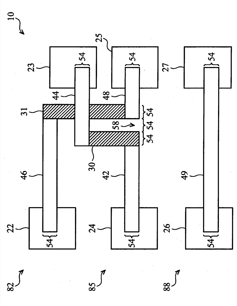
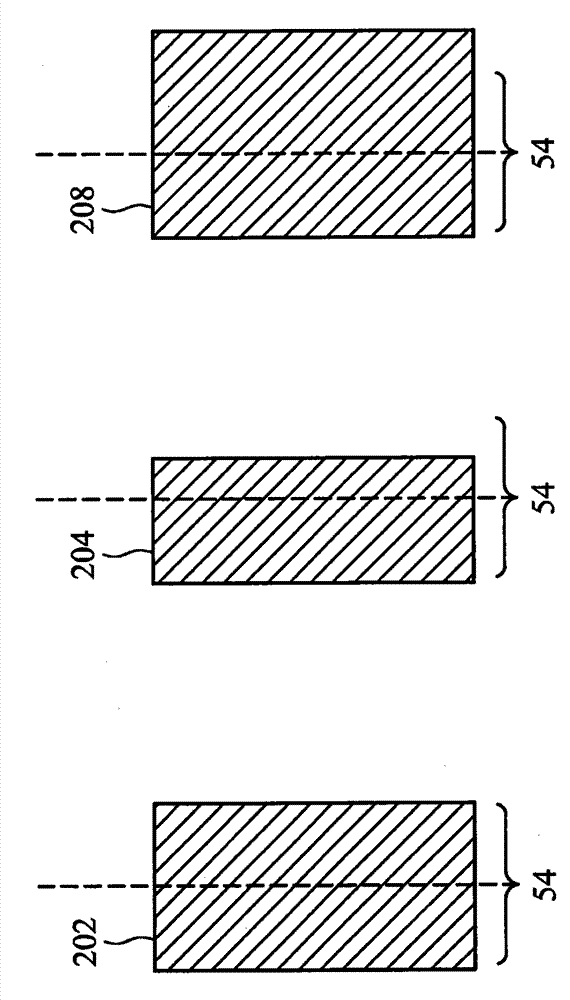
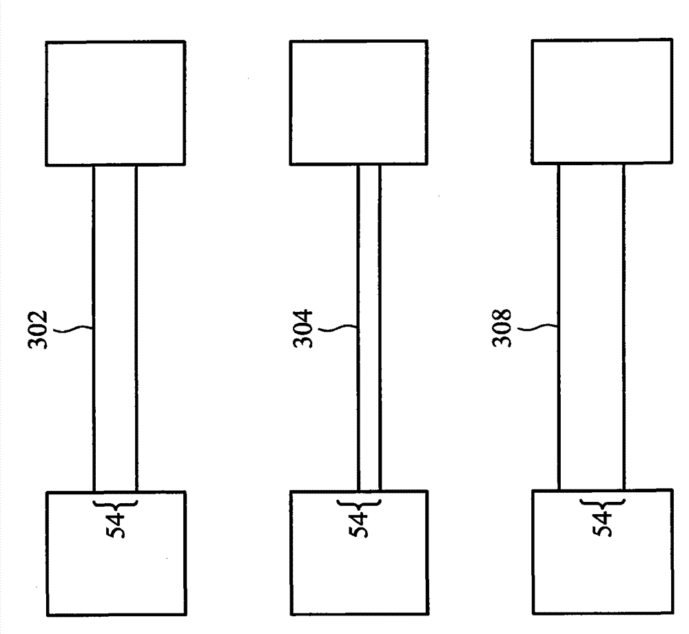
[0047] The present invention provides a method of designing an integrated circuit (IC), and in particular, provides for defining changes in critical dimensions for metal components of the IC during IC design. It should be understood, however, that the specific embodiments of the present invention are provided for teaching broader inventive concepts and that those skilled in the art will be able to apply the teachings of the present invention to other methods or apparatus. In addition, it should be understood that the methods and apparatus discussed herein include some well-known structures and / or steps. Since these structures and procedures are well known, they are discussed on a general level only. Furthermore, the repeated reference numerals in the drawings are used for illustration only, and are not used to represent any necessary combination of technical features or steps.

[0048] figure 1 A schematic diagram of a specific embodiment of the IC design 10 . IC design in...


PUM


Abstract

A method of designing an integrated circuit (IC) is provided that includes placing an IC design, where the IC design includes a first element, a second element, and a path coupling the first and second elements, and routing the IC design. Further, the method includes obtaining at least one of resistivity data and capacitance data related to the path, and obtaining timing data related to the path. The method also includes using at least one of the resistivity data, the capacitance data, and the timing data to determine a critical dimension (CD) bias to be applied to the path, and modifying the IC design, where modifying includes applying the CD bias to the path.

Description

technical field [0001] The present invention relates to methods of designing integrated circuits (ICs), and more particularly to defining critical dimension variations for metal components of the IC during IC design. Background technique [0002] Computer-Aided Design (CAD) tools can improve the efficiency of the IC design process. For example, by creating a virtual circuit layout, CAD tools help IC designers define the physical circuit layout. For example, IC designers use CAD tools to define paths and route IC components. For example, CAD tools also help IC designers perform timing analysis. [0003] In the design of an IC, one or more metal components may be included. Traditionally, the design rules for IC design use a fixed line width and a fixed spacing between two metal elements. For example, the above design rule is an equal ratio rule (50-50 ratiorule; hereinafter referred to as equal ratio rule) in which the width of each metal element is equal to the distance b...

Claims


Application Information

Patent Timeline
Patent Type & Authority Patents(China)
IPC IPC(8): G06F17/50
CPCG06F17/5072G06F2217/84G06F17/5077G06F17/5036G06F17/5031G06F30/3312G06F30/392G06F30/394G06F2119/12G06F30/367G06F30/3315
Inventor 刘潮权鲁立忠辜耀进
Owner TAIWAN SEMICON MFG CO LTD
Why Eureka
Try Eureka