Lateral Diffused Metal-Oxide-Semiconductor Device

a metal-oxide-semiconductor and lateral diffusion technology, which is applied in the direction of semiconductor devices, electrical equipment, transistors, etc., can solve the problems that the reverse source current through the parasitic diode cannot meet recent requirements and the energy loss of the ldmos device is generated, so as to save the area of the ldmos device and effectively utilize the region surrounded

Active Publication Date: 2013-07-04
MARLIN SEMICON LTD
View PDF3 Cites 27 Cited by
  • Summary
  • Abstract
  • Description
  • Claims
  • Application Information

AI Technical Summary

Benefits of technology

[0010]The LDMOS device in the present invention disposes the contact metal of the Schottky diode on the N-type first doped region at a side of the P-type second doped region extending out along the long axis to effectively utilize the region surrounded by the guard ring without affecting the current and to save the area of the LDMOS device. In addition, the LDMOS device of the present invention may further utilize the built-in Schottky diode to raise the current of the reverse current path from the source to the drain so as to accelerate the speed of introducing the reverse source current.

Problems solved by technology

Although the parasitic diode provides a reverse current path from source to drain in order to introduce minor charges, the area and the transferring speed of the reverse current path are too small to eliminate the reverse source current rapidly, so that an energy loss of the LDMOS device is generated when switching the LDMOS device.
Thus, to eliminate the reverse source current through the parasitic diode cannot satisfy recent requirements.

Method used


Image

  • Lateral Diffused Metal-Oxide-Semiconductor Device
  • Lateral Diffused Metal-Oxide-Semiconductor Device
  • Lateral Diffused Metal-Oxide-Semiconductor Device

Examples


Embodiment Construction

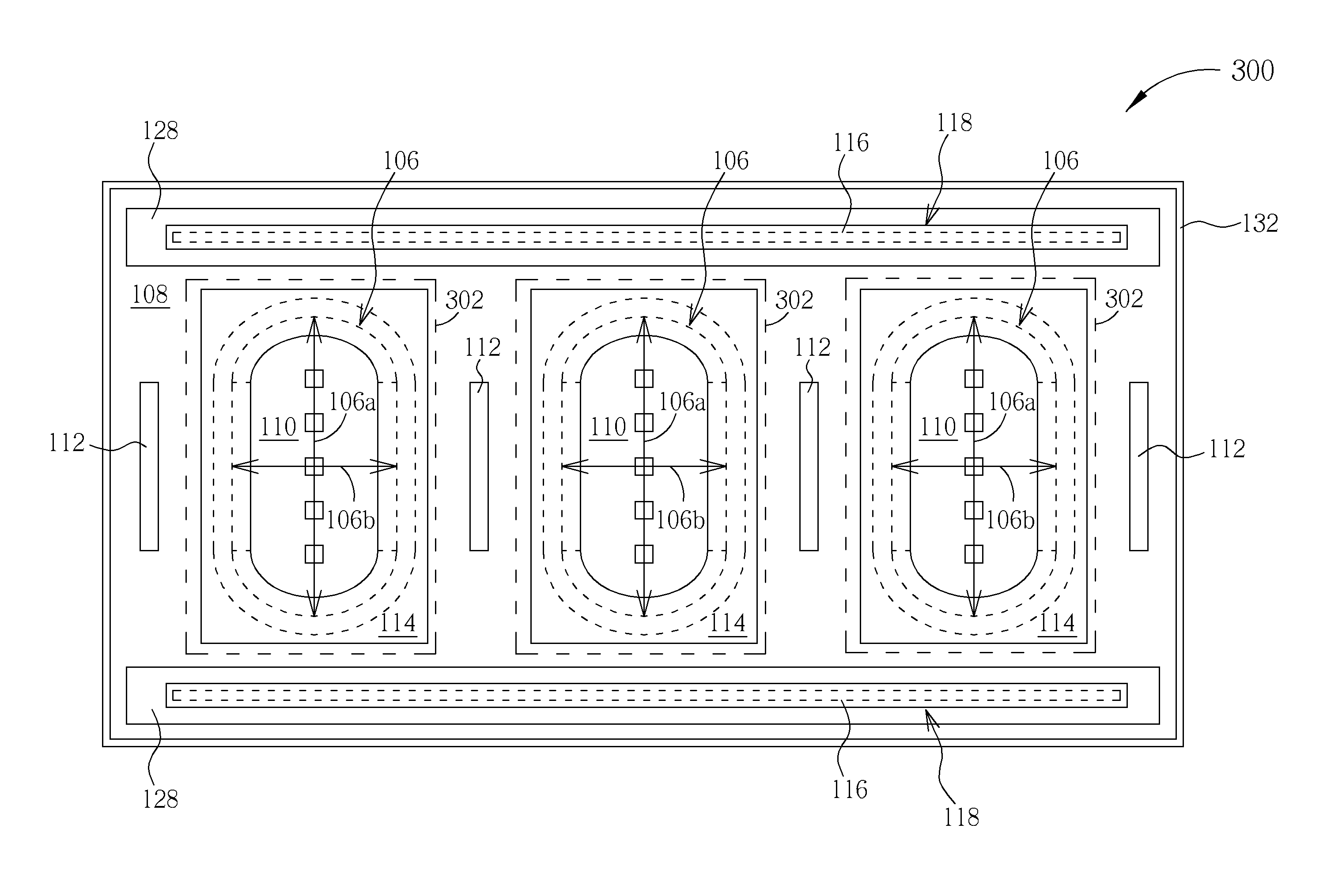
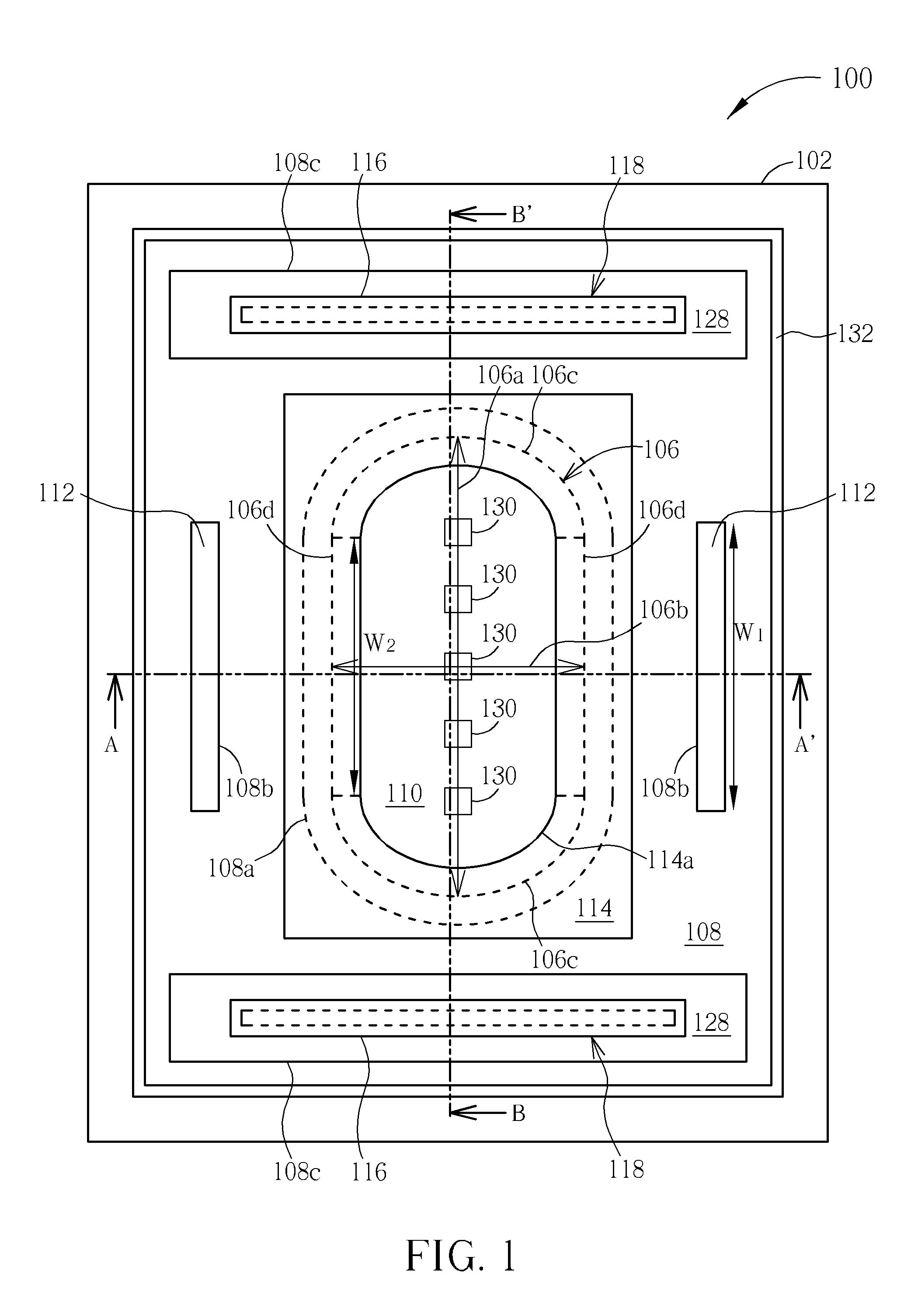
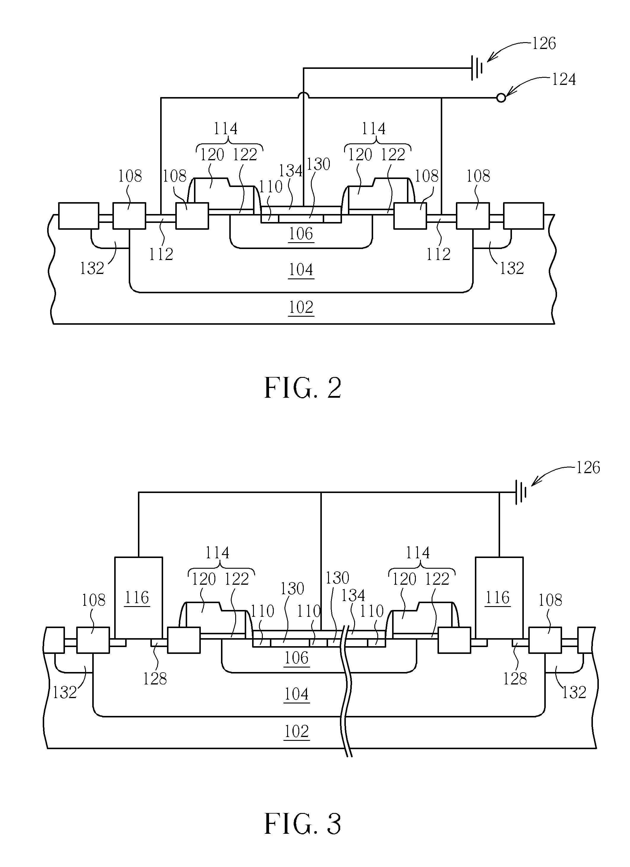
[0017]Please refer to FIG. 1 through FIG. 3. FIG. 1 is a schematic diagram illustrating a top view of a lateral diffused metal-oxide-semiconductor (LDMOS) device according to a first preferred embodiment of the present invention, wherein FIG. 2 is a schematic diagram illustrating a cross-sectional view of FIG. 1 along a cutting line A-A′, and FIG. 3 is a schematic diagram illustrating a cross-sectional view of FIG. 1 along a cutting line B-B′. As shown in FIG. 1 through FIG. 3, the LDMOS device 100 includes a substrate 102, a first doped region 104, a second doped region 106, a field oxide layer 108, a third doped region 110, two fourth doped regions 112, a gate structure 114, and a contact metal 116. The first doped region 104, the third doped region 110, and the fourth doped region have a first conductive type, and the substrate 102 and the second doped region 106 have a second conductive type different from the first conductive type. In this embodiment, the first conductive type ...


PUM


Abstract

The present invention provides a lateral diffused metal-oxide-semiconductor device including a first doped region, a second doped region, a third doped region, a gate structure, and a contact metal. The first doped region and the third doped region have a first conductive type, and the second doped region has a second conductive type. The second doped region, which has a racetrack-shaped layout, is disposed in the first doped region, and has a long axis. The third doped region is disposed in the second doped region. The gate structure is disposed on the first doped region and the second doped region at a side of the third doped region. The contact metal is disposed on the first doped region at a side of the second doped region extending out along the long axis, and is in contact with the first doped region.

Description

BACKGROUND OF THE INVENTION[0001]1. Field of the Invention[0002]The present invention relates to a lateral diffused metal-oxide-semiconductor (LDMOS) device, and more particularly, to an LDMOS device with a Schottky diode.[0003]2. Description of the Prior Art[0004]A lateral diffused metal-oxide-semiconductor (LDMOS) device is a kind of popular power semiconductor device. Due to having a planar structure, the LDMOS is easily manufactured and is easily integrated with semiconductor technology, so that the manufacturing cost may be reduced. The LDMOS further has higher breakdown voltage and higher output power so as to be applied in the devices, such as power converter, power amplifier, switch, and rectifier, etc.[0005]In a traditional LDMOS device, an N-type doped drain region and a P-type doped base region are usually disposed in an n-type drift region, and an N-type doped source region is disposed in the P-type doped base region. A gate metal is disposed on the P-type doped base reg...

Claims


Application Information

Patent Timeline
Patent Type & Authority Applications(United States)
IPC IPC(8): H01L27/06H01L29/78
CPCH01L27/0727H01L29/42368H01L29/0696H01L29/0619H01L29/782
Inventor LIN, AN-HUNGLIN, HONG-ZEHUANG, BO-JUILIAO, WEI-SHANYAN, TING-ZHOUCHOU, KUN-YICHEN, CHUN-WEIJIAN, MING-YONG
Owner MARLIN SEMICON LTD
Why Eureka
Try Eureka