Touch panel with intermediate conducting layer and manufacturing method thereof

A touch panel and conductive layer technology, applied in the direction of electrical digital data processing, input/output process of data processing, instruments, etc., can solve the problem of increasing the thickness and weight of the touch panel, large color difference of the touch panel, and alignment alignment Inaccurate and other issues, to achieve the effect of improving light transmittance and touch sensitivity, reducing etching marks, and reducing thickness and weight

Inactive Publication Date: 2010-11-24
牧东光电科技有限公司
View PDF4 Cites 8 Cited by
  • Summary
  • Abstract
  • Description
  • Claims
  • Application Information

AI Technical Summary

Problems solved by technology

[0002] Generally speaking, the processing method of touch panels adopts a layer-by-layer lamination process, which may easily cause inaccurate lamination alignment, increase the thickness and weight of the touch panel, and reduce the light transmittance and touch sensitivity of touch products. degree, it is difficult to greatly improve product quality
When processing the sensing layer, a large amount of transparent conductive material needs to be etched away to form the corresponding sensing line pattern, resulting in a large amount of etching waste liquid and serious environmental pollution; moreover, the color difference of the touch panel is large, and the etching traces are obvious

Method used


Image

  • Touch panel with intermediate conducting layer and manufacturing method thereof
  • Touch panel with intermediate conducting layer and manufacturing method thereof
  • Touch panel with intermediate conducting layer and manufacturing method thereof

Examples


Embodiment 1

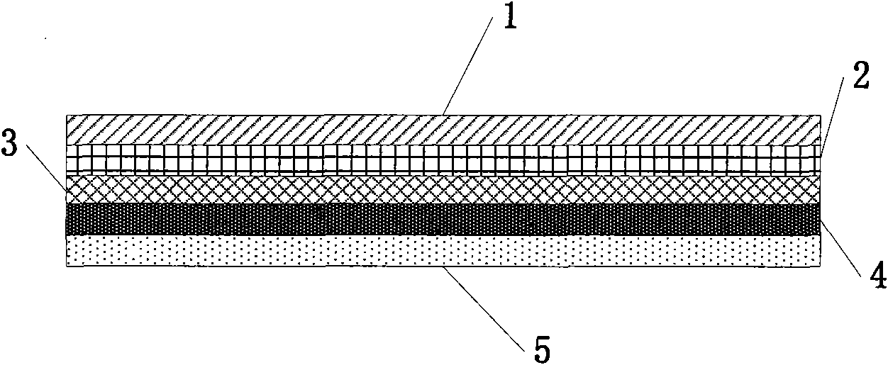
[0028] The thickness of the nameplate layer 1 is 0.7 mm; the thickness of the metal circuit layer 2 is 0.04 microns; the thickness of the middle conductive layer 3 is 0.04 microns, the thickness of the transparent conductive layer 4 is 0.04 microns; the thickness of the substrate layer 5 is 50 microns, the substrate Layer 5 is polycarbonate.

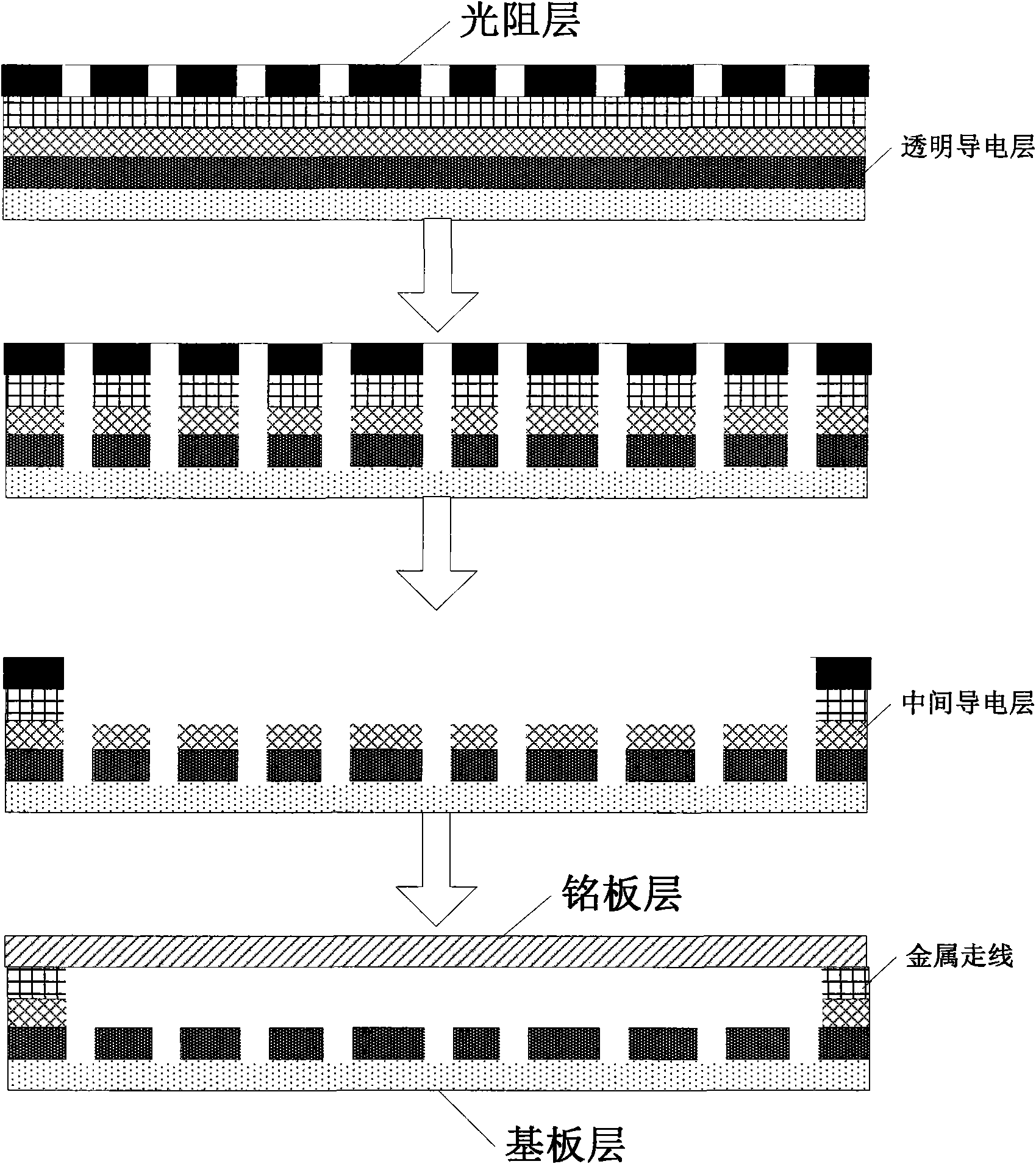
[0029] A method for manufacturing a touch panel with an intermediate conductive layer, each step is carried out under dust-free and dry conditions;

[0030] Step 1: One side of the substrate layer 5 is covered with the transparent conductive layer 4, and the intermediate conductive layer 3 is covered on the transparent conductive layer 4;

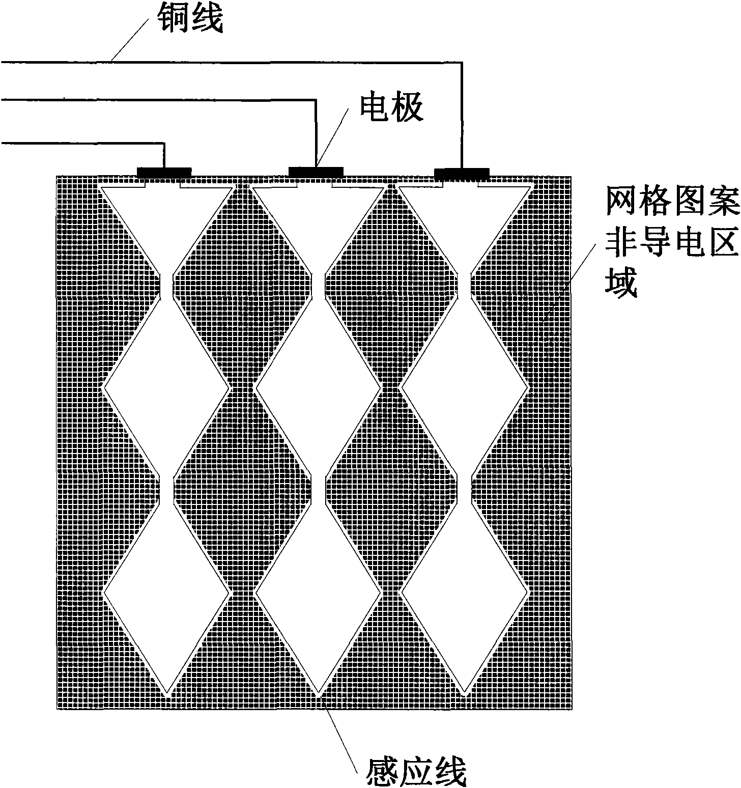
[0031] Step 2: electroplate the metal circuit layer 2 on the middle conductive layer 3, and paste a photoresist film on the metal circuit layer 2; wherein, the hollow pattern on the photoresist film matches the traces of the metal traces and the traces of the grid-shaped etching lines;

[0032] Step ...

Embodiment 2

[0037] The thickness of nameplate layer 1 is 1.8 mm; the thickness of metal circuit layer 2 is 0.07 microns; the thickness of intermediate conductive layer 3 is 0.08 microns, the thickness of transparent conductive layer 4 is 0.08 microns; the thickness of substrate layer 5 is 180 microns, the substrate Layer 5 is hardened glass.

[0038] A method for manufacturing a touch panel with an intermediate conductive layer, each step is carried out under dust-free and dry conditions;

[0039] Step 1: One side of the substrate layer 5 is covered with the transparent conductive layer 4, and the intermediate conductive layer 3 is covered on the transparent conductive layer 4;

[0040] Step 2: electroplate the metal circuit layer 2 on the middle conductive layer 3, and paste a photoresist film on the metal circuit layer 2; wherein, the hollow pattern on the photoresist film matches the traces of the metal traces and the traces of the grid-shaped etching lines;

[0041] Step 3: After exp...

Embodiment 3

[0046] The thickness of the nameplate layer 1 is 1.1 mm; the thickness of the metal circuit layer 2 is 0.1 microns; the thickness of the middle conductive layer 3 is 0.1 microns, the thickness of the transparent conductive layer 4 is 0.1 microns; the thickness of the substrate layer 5 is 125 microns, the substrate Layer 5 is polycarbonate.

[0047] A method for manufacturing a touch panel with an intermediate conductive layer, each step is carried out under dust-free and dry conditions;

[0048] Step 1: One side of the substrate layer 5 is covered with the transparent conductive layer 4, and the intermediate conductive layer 3 is covered on the transparent conductive layer 4;

[0049] Step 2: electroplating the metal circuit layer 2 on the middle conductive layer 3, and pasting a photoresist film on the metal circuit layer 2; wherein, the hollow pattern on the photoresist film coincides with the traces of the metal traces and the traces of the grid-shaped etching lines;

[00...


PUM

PropertyMeasurementUnit
Thicknessaaaaaaaaaa
Thicknessaaaaaaaaaa
Thicknessaaaaaaaaaa

Abstract

The invention discloses a touch panel with an intermediate conducting layer and a manufacturing method thereof, belonging to the technical field of a touch panel composite layer structure and manufacturing procedure thereof. In the invention, a grid pattern non-conduction region is introduced in the process of etching a sensing layer, thereby reducing etching spent liquor and being favor for environmental protection; and in the process of processing the touch panel, a light resistance etching technology is fully utilized to carry out allopelagic bedding surface precision finishing on the touch panel, and an intermediate conducting layer is additionally arranged to play roles in protecting conducting material and improving the adhesive force of the conducting materials.

Description

technical field [0001] The invention relates to a touch panel with an intermediate conductive layer and a manufacturing method thereof, and belongs to the technical field of touch panel composite layer structure and its manufacturing process. Background technique [0002] Generally speaking, the processing method of touch panels adopts a layer-by-layer lamination process, which may easily cause inaccurate lamination alignment, increase the thickness and weight of the touch panel, and reduce the light transmittance and touch sensitivity of touch products. It is difficult to greatly improve product quality. When processing the sensing layer, a large amount of transparent conductive material needs to be etched away to form the corresponding sensing line pattern, resulting in a large amount of etching waste liquid and serious environmental pollution; moreover, the color difference of the touch panel is large and the etching marks are obvious. [0003] With the continuous develo...

Claims


Application Information

Patent Timeline
IPC IPC(8): G06F3/041
CPCG06F2203/04103G06F3/041G06F2203/04112
Inventor 陈栋南
Owner 牧东光电科技有限公司
Why Eureka
Try Eureka