Large touch panel with through holes and manufacture method thereof
A touch panel, large-scale technology, applied in the direction of instruments, electrical digital data processing, data processing input/output process, etc., can solve electronic mechanism failures, affect the operation of the touch panel, easy to generate air bubbles, load changes and Newton Ring and other problems, to achieve the effect of improving support force, penetrating force and sensitivity, and low production cost
- Summary
- Abstract
- Description
- Claims
- Application Information
AI Technical Summary
Problems solved by technology
Method used
Image
Examples
Embodiment 1
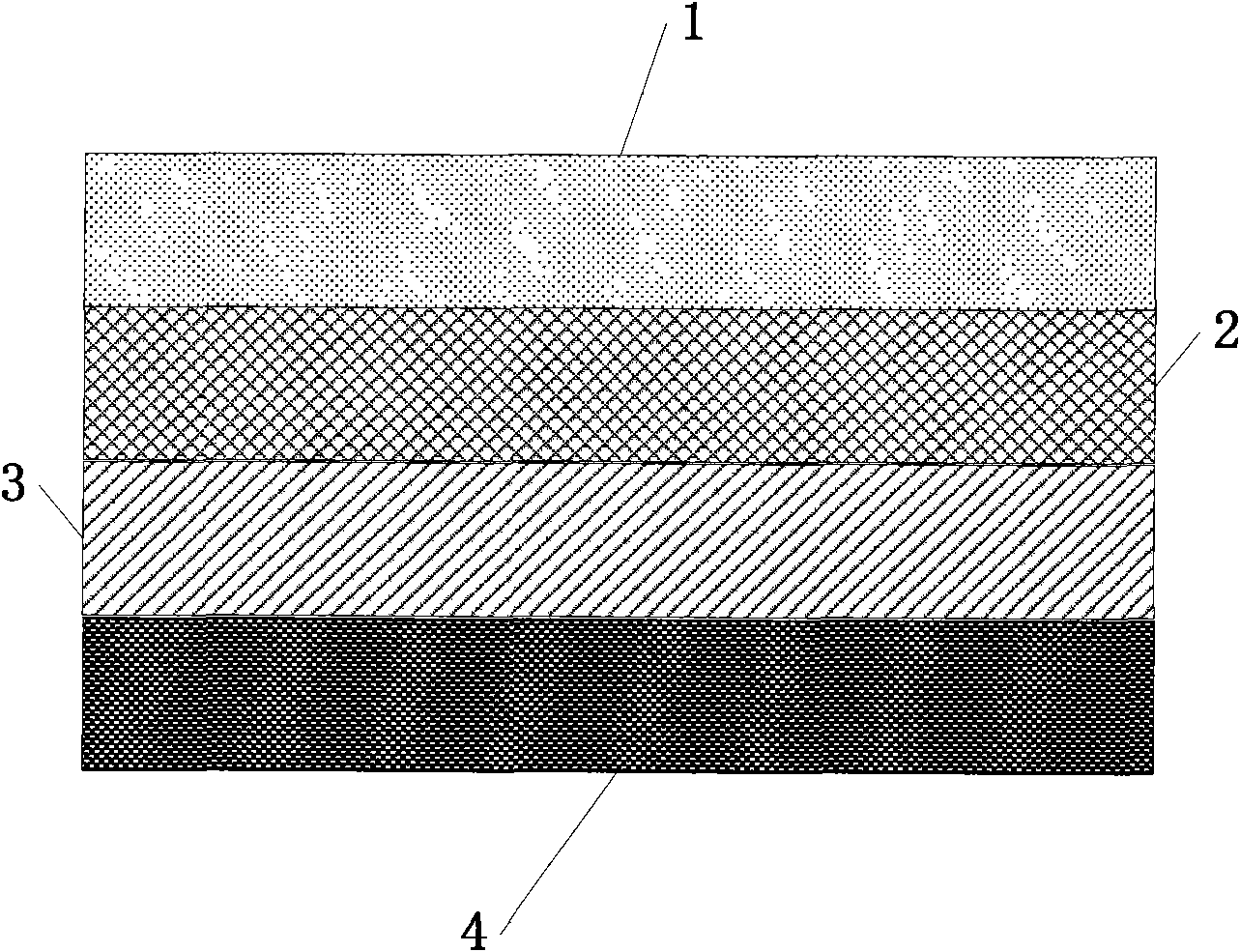
[0027] The thickness of the nameplate layer 1 is 0.125 mm; the thickness of the upper conductive pattern layer 2 and the lower conductive pattern layer 3 is 0.045 mm; the thickness of the substrate layer 4 is 0.3 mm, and the substrate layer 4 is hardened glass.
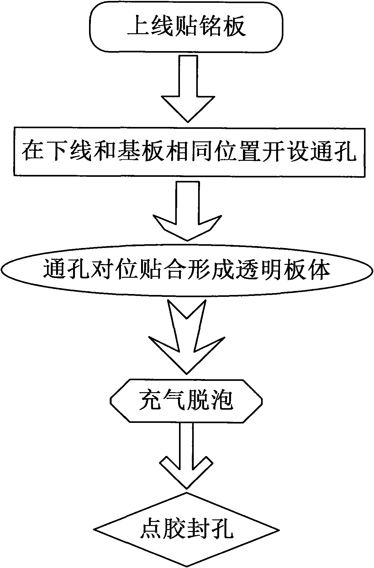
[0028] The method for manufacturing a large-size touch panel with a through hole, the following steps are carried out under dust-free and dry conditions:
[0029] Step 1: The nameplate layer 1 is attached to the upper line conductive pattern layer 2;
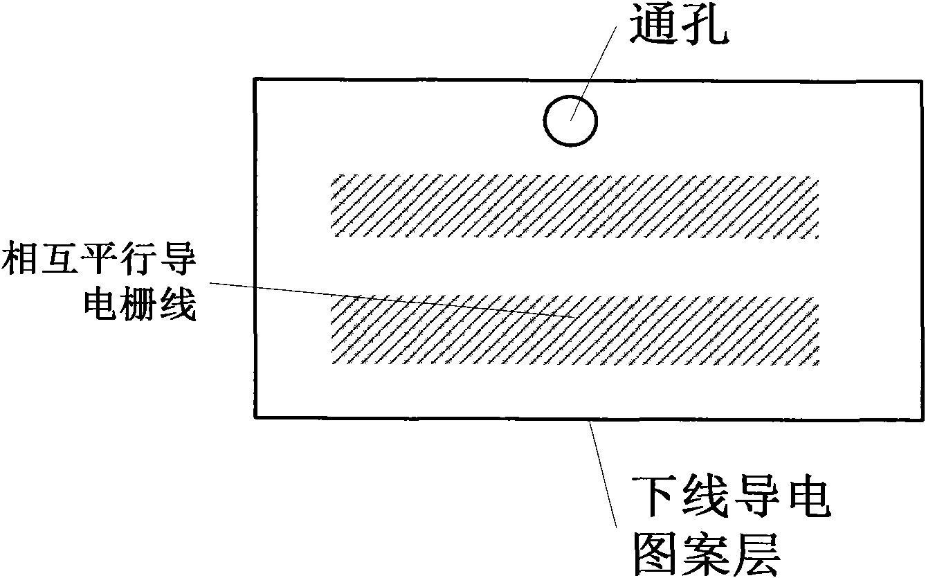
[0030] Step 2: Through the middle position of the lower conductive pattern layer 3 and the peripheral part of the substrate layer 4, the laser laser obtains a through hole; the through hole of the lower conductive pattern layer 3 and the through hole of the substrate layer 4 are aligned, and the lower conductive pattern layer 3 and the through hole of the substrate layer 4 are aligned. Lamination of substrate layer 4;
[0031] Step 3: The lower-line conductive pattern ...
Embodiment 2
[0035] The thickness of the nameplate layer 1 is 0.188 mm; the thickness of the upper conductive pattern layer 2 and the lower conductive pattern layer 3 is 0.188 mm; the thickness of the substrate layer 4 is 2.5 mm, and the substrate layer 4 is polycarbonate resin.
[0036] The method for manufacturing a large-size touch panel with a through hole, the following steps are carried out under dust-free and dry conditions:
[0037] Step 1: The nameplate layer 1 is attached to the upper line conductive pattern layer 2;
[0038] Step 2: Through the middle position of the lower conductive pattern layer 3 and the peripheral part of the substrate layer 4, the laser laser obtains a through hole; the through hole of the lower conductive pattern layer 3 and the through hole of the substrate layer 4 are aligned, and the lower conductive pattern layer 3 and the through hole of the substrate layer 4 are aligned. Lamination of substrate layer 4;
[0039] Step 3: The lower-line conductive pat...
Embodiment 3
[0043] The thickness of the nameplate layer 1 is 0.158 mm; the thickness of the upper conductive pattern layer 2 and the lower conductive pattern layer 3 is 0.128 mm; the thickness of the substrate layer 4 is 1.8 mm, and the substrate layer 4 is hardened glass.
[0044] The method for manufacturing a large-size touch panel with a through hole, the following steps are carried out under dust-free and dry conditions:
[0045] Step 1: The nameplate layer 1 is attached to the upper line conductive pattern layer 2;
[0046] Step 2: Through the middle position of the lower conductive pattern layer 3 and the peripheral part of the substrate layer 4, the laser laser obtains a through hole; the through hole of the lower conductive pattern layer 3 and the through hole of the substrate layer 4 are aligned, and the lower conductive pattern layer 3 and the through hole of the substrate layer 4 are aligned. Lamination of substrate layer 4;
[0047] Step 3: The lower-line conductive pattern ...
PUM
 Abstract
Description
Claims
Application Information


