Method for externally expanding single edge of circuit of touch panel
A touch panel, unilateral technology, used in chemical/electrolytic methods to remove conductive materials, data processing input/output processes, instruments, etc. The effect of electrical signal transmission, strong operation controllability, and reduction of manufacturing costs
- Summary
- Abstract
- Description
- Claims
- Application Information
AI Technical Summary
Problems solved by technology
Method used
Image
Examples
Embodiment 1
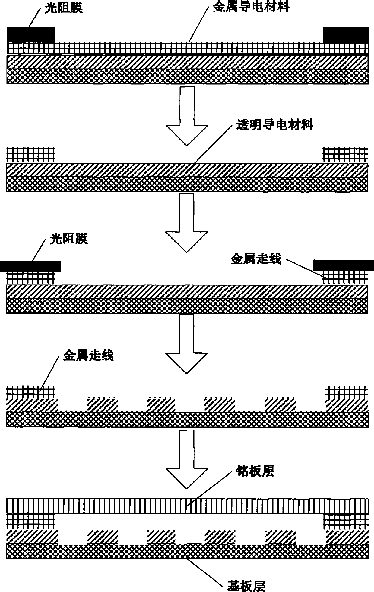
[0023] The thickness of the nameplate layer is 0.7 mm; the thickness of the metal conductive material is 0.05 micron; the thickness of the transparent conductive material is 0.045 micron; the thickness of the substrate layer is 50 micron, and the substrate layer is polycarbonate resin.
[0024] The method for unilateral expansion of the touch panel circuit includes the following steps to be carried out under dust-free and dry conditions;
[0025] Step 1: electroplating metal conductive material on the surface of transparent conductive material;
[0026] Step 2: paste a photoresist film on the metal conductive material, expose, develop and etch to form a metal trace; at room temperature, etch the metal conductive material with a mixed solution of sulfuric acid and hydrogen peroxide to obtain a metal trace;
[0027] Step 3: first attach a photoresist film on the metal traces, wherein the width of the photoresist film on a single metal trace is 65 microns; then, expose and develo...
Embodiment 2
[0031] The thickness of the nameplate layer is 1.8 mm; the thickness of the metal conductive material is 0.1 micron; the thickness of the transparent conductive material is 0.1 micron; the thickness of the substrate layer is 180 micron, and the substrate layer is hardened glass.
[0032] The method for unilateral expansion of the touch panel circuit includes the following steps to be carried out under dust-free and dry conditions;
[0033] Step 1: electroplating metal conductive material on the surface of transparent conductive material;
[0034] Step 2: paste a photoresist film on the metal conductive material, expose, develop and etch to form a metal trace; at room temperature, etch the metal conductive material with a mixed solution of sulfuric acid and hydrogen peroxide to obtain a metal trace;
[0035] Step 3: first attach a photoresist film on the metal traces, wherein the width of the photoresist film on a single metal trace is 75 microns; then, expose and develop to et...
Embodiment 3
[0039] The thickness of the nameplate layer is 1.1 mm; the thickness of the metal conductive material is 0.09 microns; the thickness of the transparent conductive material is 0.08 microns; the thickness of the substrate layer is 125 microns, and the substrate layer is polycarbonate resin.
[0040] The method for unilateral expansion of the touch panel circuit includes the following steps to be carried out under dust-free and dry conditions;
[0041] Step 1: electroplating metal conductive material on the surface of transparent conductive material;
[0042] Step 2: paste a photoresist film on the metal conductive material, expose, develop and etch to form a metal trace; at room temperature, etch the metal conductive material with a mixed solution of sulfuric acid and hydrogen peroxide to obtain a metal trace;
[0043] Step 3: first attach a photoresist film on the metal traces, wherein the width of the photoresist film on a single metal trace is 70 microns; then, expose and dev...
PUM
| Property | Measurement | Unit |
|---|---|---|
| thickness | aaaaa | aaaaa |
| thickness | aaaaa | aaaaa |
| thickness | aaaaa | aaaaa |
Abstract
Description
Claims
Application Information


