Method of manufacturing grid pattern type touch panel

A touch panel and grid manufacturing technology, applied in the input/output process of data processing, instruments, electrical digital data processing, etc. Inaccurate positioning and other issues, to achieve the effect of improving light transmittance and touch sensitivity, reducing etching marks, and reducing thickness and weight

Active Publication Date: 2015-12-16
牧东光电科技有限公司
View PDF4 Cites 0 Cited by
  • Summary
  • Abstract
  • Description
  • Claims
  • Application Information

AI Technical Summary

Problems solved by technology

[0002] If the touch panel is processed in a layer-by-layer lamination process, it is easy to cause inaccurate lamination alignment, increase the thickness and weight of the touch panel, and reduce the light transmittance and touch sensitivity of the touch product. It is difficult to improve the quality
When processing transparent conductive materials, a large amount of transparent conductive materials need to be etched away to form the corresponding induction line pattern, resulting in a large amount of etching waste liquid and serious environmental pollution; and the color difference of the touch panel is large, and the etching marks are obvious

Method used


Image

  • Method of manufacturing grid pattern type touch panel
  • Method of manufacturing grid pattern type touch panel
  • Method of manufacturing grid pattern type touch panel

Examples


Embodiment 1

[0025] The thickness of the nameplate layer is 0.7 mm; the thickness of the metal conductive material is 0.04 microns; the thickness of the transparent conductive material is 0.045 mm; the thickness of the substrate layer is 50 microns, and the substrate layer is polycarbonate resin.

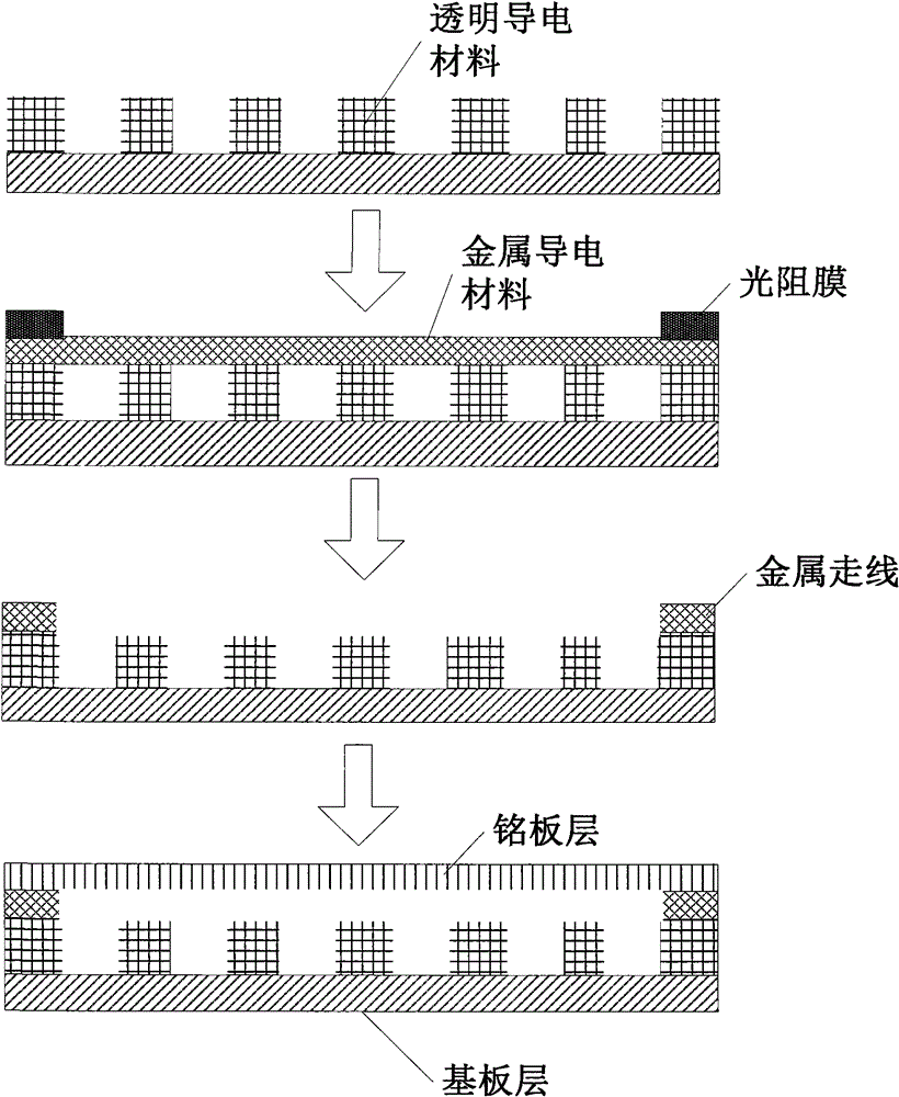
[0026] A method for manufacturing a grid-patterned touch panel, comprising the following steps carried out under dust-free and dry conditions;

[0027] Step 1: Aging crystallization of transparent conductive materials;

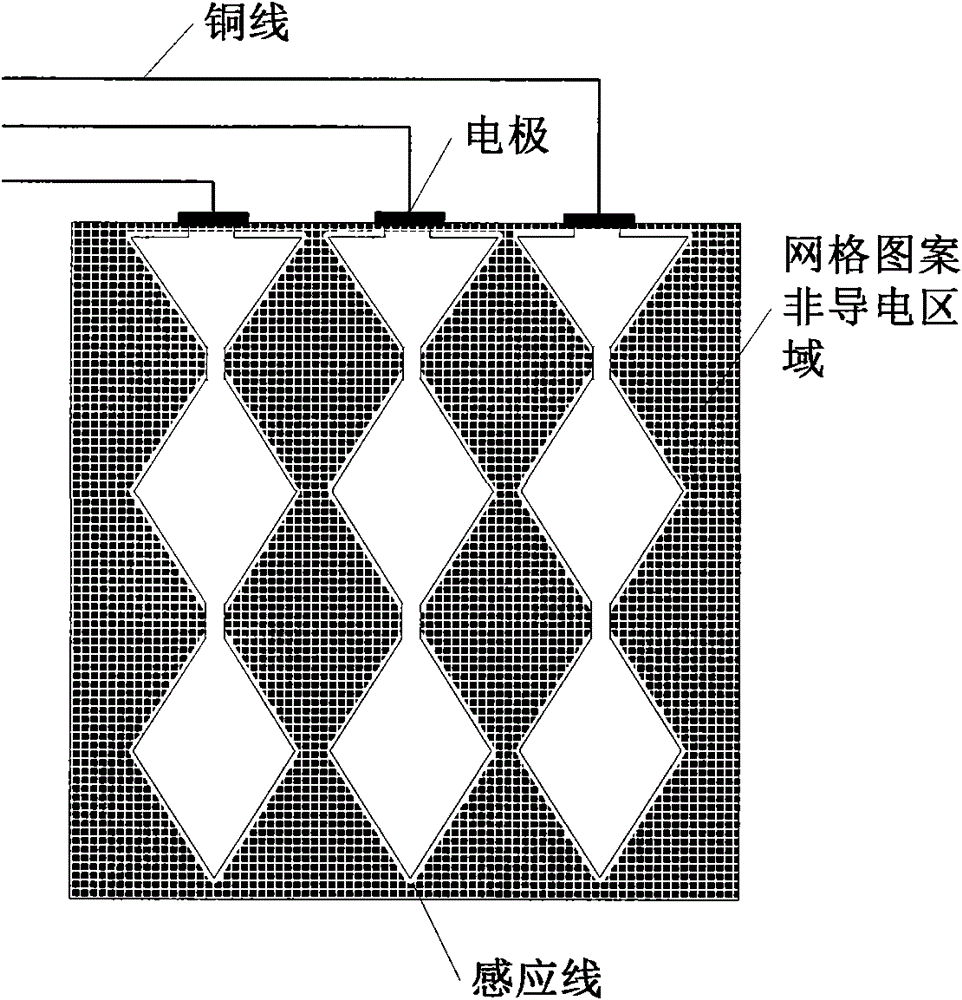
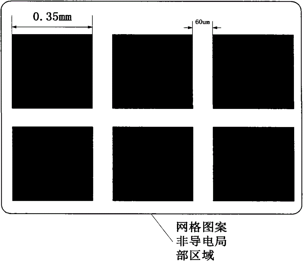
[0028] Step 2: Expose and etch the aging crystalline transparent conductive material, etch the transparent conductive material with hydrochloric acid at a temperature of 40 degrees Celsius to form a non-conductive area of ​​induction lines and grid patterns;

[0029] Step 3: In step 2, the surface of the transparent conductive material is electroplated with a metal conductive material;

[0030] Step 4: paste a photoresist film on the metal conductive material, expose, develop a...

Embodiment 2

[0034] The thickness of the nameplate layer is 1.8 mm; the thickness of the metal conductive material is 0.1 micron; the thickness of the transparent conductive material is 0.1 micron; the thickness of the substrate layer is 180 micron, and the substrate layer is hardened glass.

[0035] A method for manufacturing a grid-patterned touch panel, comprising the following steps carried out under dust-free and dry conditions;

[0036] Step 1: Aging crystallization of transparent conductive materials;

[0037] Step 2: Expose and etch the aging crystalline transparent conductive material, etch the transparent conductive material with hydrochloric acid at a temperature of 40 degrees Celsius to form a non-conductive area of ​​induction lines and grid patterns;

[0038] Step 3: In step 2, the surface of the transparent conductive material is electroplated with a metal conductive material;

[0039] Step 4: paste a photoresist film on the metal conductive material, expose, develop and et...

Embodiment 3

[0043] The thickness of the nameplate layer is 1.1 mm; the thickness of the metal conductive material is 0.08 microns; the thickness of the transparent conductive material is 0.07 microns; the thickness of the substrate layer is 125 microns, and the substrate layer is polycarbonate resin.

[0044] A method for manufacturing a grid-patterned touch panel, comprising the following steps carried out under dust-free and dry conditions;

[0045] Step 1: Aging crystallization of transparent conductive materials;

[0046] Step 2: Expose and etch the aging crystalline transparent conductive material, etch the transparent conductive material with hydrochloric acid at a temperature of 40 degrees Celsius to form a non-conductive area of ​​induction lines and grid patterns;

[0047] Step 3: In step 2, the surface of the transparent conductive material is electroplated with a metal conductive material;

[0048] Step 4: paste a photoresist film on the metal conductive material, expose, deve...


PUM

PropertyMeasurementUnit
thicknessaaaaaaaaaa
thicknessaaaaaaaaaa
thicknessaaaaaaaaaa

Abstract

Disclosed is a method for manufacturing a touch panel of the grid-pattern type, comprising the steps of: etching a transparent conductive material to form nonconductive regions in a grid pattern by using photoresist technology, then electroplating a metallic conductive material thereon, affixing a photoresist film onto the metallic conductive material, and forming metal wiring by exposing, developing and etching thereon. The method can reduce the etching traces, and decrease the etching waste liquid so that it is beneficial for environmental protection, and it is simple to operate, which can reduce manufacturing costs.

Description

technical field [0001] The invention relates to a method for manufacturing a grid pattern touch panel, which belongs to the technical field of touch panel manufacturing. Background technique [0002] If the touch panel is processed in a layer-by-layer lamination process, it is easy to cause inaccurate lamination alignment, increase the thickness and weight of the touch panel, and reduce the light transmittance and touch sensitivity of the touch product. It is difficult to greatly improve the quality. When processing transparent conductive materials, a large amount of transparent conductive materials need to be etched away to form the corresponding sensing line pattern, resulting in a large amount of etching waste liquid and serious environmental pollution; moreover, the color difference of the touch panel is large and the etching marks are obvious. [0003] The present invention can perform photoresist etching on different depth layers of the touch panel by adopting photore...

Claims


Application Information

Patent Timeline
Patent Type & Authority Patents(China)
IPC IPC(8): G06F3/041
CPCG06F3/041G06F2203/04103G06F2203/04112
Inventor 陈栋南
Owner 牧东光电科技有限公司
Why Eureka
Try Eureka