Method for processing round arrays by electronic beam photo-etching

A technology of electron beam lithography and circular array, applied in the field of nanofabrication, can solve the problems of increasing the cost of pattern processing, and achieve the effect of being easy to understand and shortening the time spent

Inactive Publication Date: 2010-12-15
SUZHOU INST OF NANO TECH & NANO BIONICS CHINESE ACEDEMY OF SCI
View PDF5 Cites 5 Cited by
  • Summary
  • Abstract
  • Description
  • Claims
  • Application Information

AI Technical Summary

Problems solved by technology

[0003] However, due to the regular array pattern of round holes or cylinders, the cost of pattern processing will be greatly increased if the original technical method is not utilized.

Method used


Image

  • Method for processing round arrays by electronic beam photo-etching
  • Method for processing round arrays by electronic beam photo-etching
  • Method for processing round arrays by electronic beam photo-etching

Examples


Embodiment 1

[0022] Taking silicon as the sample to be processed (hereinafter referred to as silicon substrate), it needs to be formed on the sample figure 1 In the shown double-row / / circular hole array with a period of 100 nm and a diameter of 30 nm, the interval between the array and the array is 600 nm, and the array length is 10 μm.

[0023] (1) Graphic design, draw a rectangle (length 10μm, width 200nm), the interval between the rectangle and the rectangle is 600nm.

[0024] (2) After necessary cleaning, the silicon substrate is coated with PMMA A4 photoresist at a process parameter of 4000 revolutions per minute, then baked on a hot plate for 90 seconds, and then cooled for another 2 minutes.

[0025] (3) Perform electron beam exposure on the sample, using JBX5500ZA electron beam lithography machine, beam current 100pA, exposure dose 200μC / cm2, scanning step length 100nm.

[0026] (4) Take out the sample, develop with MIBK:IPA for 90 seconds, and fix with IPA for 30 seconds to form the desi...

Embodiment 2

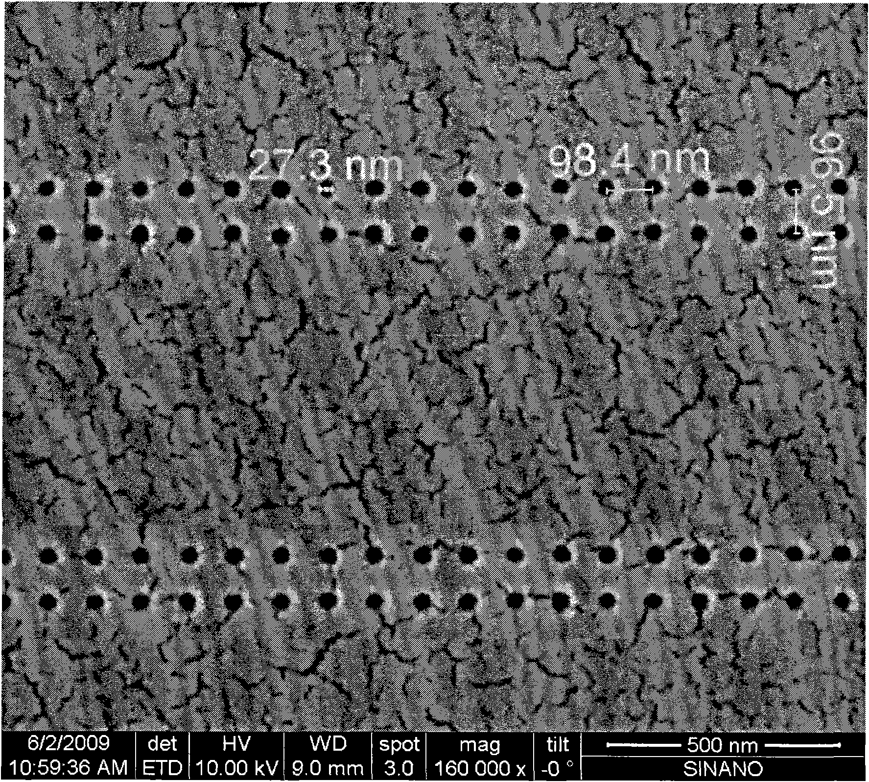
[0028] The same sample to be processed needs to be formed on the sample figure 2 Shown is an array of circular holes with a diameter of 55 nm and a period of 100 nm.

[0029] (1) Graphic design, first draw a rectangle on the silicon substrate (according to the size of the circular hole array, no specific size is specified here).

[0030] (2) After necessary cleaning of the substrate silicon, PMMAA4 photoresist is coated with a process parameter of 4000 revolutions per minute, and then baked on a hot plate for 90 seconds, and then cooled for 2 minutes.

[0031] (3) Perform electron beam exposure on the sample, using JBX5500ZA electron beam lithography machine, beam current 100pA, exposure dose 500μC / cm 2 , The scanning step is 100nm.

[0032] (4) Take out the sample, use MIBK: IPA to develop for 90s, and IPA to fix for 30s to form the desired pattern.

Embodiment 3

[0034] The same sample to be processed needs to be formed on the sample image 3 The three rows shown are an array of circular holes with a period of 50 nm and a diameter of about 20 nm.

[0035] (1) Graphic design, first draw a rectangle on the silicon substrate (depending on the size of the circular hole array, 10μm in length and 150nm in width), with an interval of 50nm between the rectangle and the rectangle.

[0036] (2) After necessary cleaning, the substrate silicon is coated with PMMAA4 photoresist at a process parameter of 4000 revolutions per minute, and then baked on a hot plate for 90 seconds, and then cooled for another 2 minutes.

[0037] (3) Perform electron beam exposure on the sample, using JBX5500ZA electron beam lithography machine, beam current 100pA, exposure dose 200μC / cm 2 , The scanning step is 50nm.

[0038] (4) Take out the sample, develop with MIBK:IPA for 90 seconds, and fix with IPA for 30 seconds to form the desired pattern.


PUM


Abstract

The invention relates to a method for processing round arrays by electronic beam photo-etching and aims to reduce data volume when arc-shaped lines are processed and shorten data processing time. The characteristics of the working mode of a Guass type beam spot vector scanning electronic beam photo-etching machine are fully utilized and a specific scanning step length and exposure dose are set to obtain round porous or columnar nano arrays with different diameters and different intervals, wherein a minimum clearance between patterns can be 10 nanometers. The method can be used for processing the round porous or columnar nano arrays with different diameters and different intervals, wherein the minimum clearance between patterns can be 10 nanometers. Compared with the conventional method for directly processing the round arrays, the technical method has the most outstanding advantage that: circular-arc pattern data does not need to be used in an entire flow, so that time consumed by data processing is shortened greatly.

Description

Technical field [0001] The present invention relates to nano processing technology, in particular to a method for processing a nano-level circular array on a specific material, wherein the so-called circular array is an array structure of any shape formed by circular holes or cylinders. Background technique [0002] Electron beam lithography does not require a mask, and can design processing patterns of any shape through software, which is flexible and convenient to use; and it has extremely fine processing capabilities. At present, 10nm lines have been obtained through this technology. At present, electron beam lithography is increasingly used in the processing of nano-patterns. However, for many arc-shaped nano-lines, in the data processing process before exposure, it is generally necessary to use a large number of rectangles to infinitely approximate the arc-shaped lines, resulting in The amount of processed data is huge, and it takes a lot of time for data processing, which g...

Claims


Application Information

Patent Timeline
IPC IPC(8): G03F7/00G03F7/20
Inventor时文华钟飞王逸群曾春红董艳周健
OwnerSUZHOU INST OF NANO TECH & NANO BIONICS CHINESE ACEDEMY OF SCI