Dielectric layer

A dielectric layer and silicide technology, applied in circuits, electrical components, transistors, etc., can solve problems that affect component characteristics, increase interface defects, and difficulties, and achieve the effect of improving component characteristics and improving component characteristics

Inactive Publication Date: 2010-12-15
AU OPTRONICS CORP
View PDF0 Cites 2 Cited by
  • Summary
  • Abstract
  • Description
  • Claims
  • Application Information

AI Technical Summary

Problems solved by technology

Especially after the subsequent ion implantation (Ion Implant) process, the grain boundary defects (grain boundary traps) and oxide layer interface defects in the polysilicon layer and the interface defects (interface trap states) between the polysilicon layer and the gate insulating layer increase , and the gate insulating film produces many dangling bonds, increasing the chance of charged particles being confined, thereby affecting the characteristics of the device
[0005] Based on the above, under the original polysilicon thin film transistor technology, it becomes very difficult to further improve the component characteristics of the polysilicon thin film transistor technology

Method used


Image

  • Dielectric layer
  • Dielectric layer
  • Dielectric layer

Examples


Embodiment 1

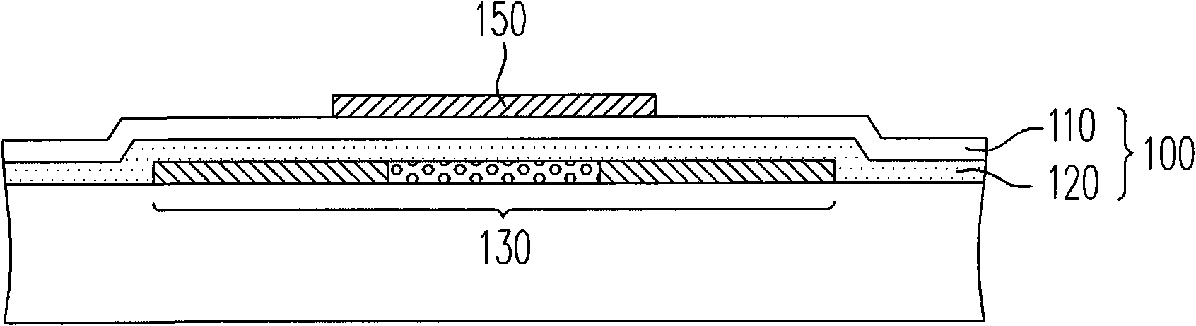
[0050] figure 1 It is a schematic diagram of applying a dielectric layer proposed by the present invention to a thin film transistor. Please refer to figure 1 In this embodiment, the dielectric layer 100 includes the oxygen-containing silicide film 120 and the nitrogen-containing silicide film 110 as an example. In this embodiment, the nitrogen-containing silicide film 110 is, for example, a nitrogen source, such as: laughing gas (N 2 O) and silicon sources, such as: silane (SiH 4 ) is a reactive gas, which is formed by a chemical vapor deposition process, but is not limited to these reactive gases, and other reactive gases can also be used selectively, for example: nitrogen source (such as: nitrogen, ammonia, nitrogen / ammonia mixture, Nitrogen / laughing gas mixture, laughing gas, or other gases, or mixtures of the above) and silicon sources (such as: disilane, tetramethylsilane, tetramethoxysilane, tetraethoxysilane, or other gases, or combinations of the above). By adjus...

Embodiment 2

[0056] The present invention further proposes a thin film transistor 200 comprising a substrate 202, an active layer 210, a first dielectric layer 220, a gate 250, a second dielectric layer 260, a source region 212 / drain region 214 , a third dielectric layer 290 and a pixel electrode 292 . The active layer 210 is disposed on the substrate 202 and has a source region 212 , a drain region 214 and a channel region 216 between the source region 212 and the drain region 214 . The first dielectric layer 220 is disposed on the substrate 202 to cover the active layer 210 . The gate 250 is disposed on a part of the first dielectric layer 220 . The second dielectric layer 260 is disposed on the substrate 202 and covers the gate 250 . The source 270 / drain 280 are disposed on part of the second dielectric layer 260 and electrically connected to the source region 212 / drain 214 of the active layer 210 . The third dielectric layer 290 is disposed on the substrate 202 and covers the sour...

Embodiment 3

[0063] image 3 It is a schematic diagram of another thin film transistor proposed by the present invention. Please refer to image 3 The thin film transistor 300 includes a substrate 302 , a gate 350 , a first dielectric layer 320 , an active layer 310 , a source 370 / drain 380 , a second dielectric layer 360 and a pixel electrode 392 . The gate 350 is disposed on the substrate 302 . The first dielectric layer 320 is disposed on the substrate 302 to cover the gate 350 . The active layer 310 is disposed on a part of the first dielectric layer 320, and the active layer 310 has a source region 312, a drain region 314, and a trench between the source region 312 and the drain region 314. Road District 316. The source 370 / drain 380 are connected to the source region 312 / drain 314 of the active layer 310 . The second dielectric layer 360 is disposed on the substrate 302 and covers the source 370 / drain 380 , the active layer 310 and the first dielectric layer 320 . The pixel...


PUM

PropertyMeasurementUnit
compressive stressaaaaaaaaaa

Abstract

The invention discloses a dielectric layer, comprising an oxygenic silicide film and a nitrogenous silicide film, wherein in the Fourier transformation infrared spectrum of the nitrogenous silicide film, the ratio of the absorption peak strength of Si-N base and the film thickness of the nitrogenous silicide film is more than 0.67 / mu m; and the refraction coefficient of the nitrogenous silicide film is more than 1.8 and less than 1.84. The above dielectric layer can be used in switch assemblies.

Description

[0001] The present invention is a divisional application for the parent application (application number: 200710109412.9, invention name: dielectric layer and thin film transistor). technical field [0002] The invention relates to a dielectric layer and a thin film transistor, in particular to a high-quality dielectric layer and a thin film transistor with the dielectric layer. Background technique [0003] Among many flat panel displays, thin film transistor liquid crystal displays (Thin Film Transistor Liquid Crystal Display, TFT LCD), which have superior characteristics such as high image quality, good space utilization efficiency, low power consumption, and no radiation, have become the mainstream in the display field. In particular, in the manufacture of thin-film transistor liquid crystal displays, high-quality gate insulating film formation technology affects the component characteristics of thin-film transistors. [0004] In a known polysilicon TFT process, the amorp...

Claims


Application Information

Patent Timeline
Patent Type & Authority Applications(China)
IPC IPC(8): H01L29/51H01L29/786H01L21/285
Inventor 许建宙
Owner AU OPTRONICS CORP
Why Eureka
Try Eureka