Touch plane display panel and manufacture method thereof

A manufacturing method and technology for liquid crystal display panels, which are applied to static indicators, instruments, electrical digital data processing, etc., can solve problems such as damaged components, scratches, and lowering the manufacturing yield of the integrated touch panel 100A, and achieve improved scratching. Injury or damage, the effect of improving the manufacturing yield

Inactive Publication Date: 2011-01-12
AU OPTRONICS CORP
View PDF4 Cites 22 Cited by
  • Summary
  • Abstract
  • Description
  • Claims
  • Application Information

AI Technical Summary

Problems solved by technology

[0006] As mentioned above, since the known integrated touch panels 100A and 100B have to perform 4 processes on the outer surface of the substrate 110 first, and then turn over and perform another 7 processes on the inner surface of the subst

Method used


Image

  • Touch plane display panel and manufacture method thereof
  • Touch plane display panel and manufacture method thereof
  • Touch plane display panel and manufacture method thereof

Examples


Embodiment Construction

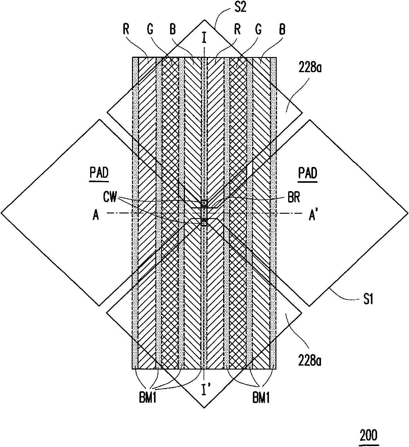
[0055] figure 2 It is a top view of a touch liquid crystal display panel according to an embodiment of the present invention. Figure 3H for figure 2 Sectional view of line A-A' in the middle. Figure 4H for figure 2 Sectional view of line I-I' in the middle. Please also refer to figure 2 , Figure 3H and Figure 4H The touch liquid crystal display panel 200 of this embodiment includes an array substrate 210 , a touch color filter substrate 220 , a liquid crystal layer 230 and a plurality of peripheral circuits (not shown). In this embodiment, the array substrate 210 is, for example, an active device array substrate. Generally speaking, the active device array substrate includes active devices, scan lines, data lines, pixel electrodes, storage capacitors and other components. The touch-sensitive color filter substrate 220 includes a substrate 222 (or referred to as a substrate), a plurality of bridging wires 224, a plurality of color filter films 226, a sensing cir...


PUM


Abstract

The invention relates to a manufacture method of a touch plane display panel, which comprises the steps of: providing a base plate provided with an outer surface and an inner surface relative to the outer surface; forming a plurality of bridge wires and a plurality of color filter films arranged in arrays on the outer surface, wherein the color filter films are provided with a plurality of touch openings; partial regions of each bridge wire are respectively exposed by two touch openings; forming a sensing line layer on the color filter films, wherein partial sensing line layers are electrically connected with the bridge wires through the touch openings; and assembling a liquid crystal layer between the inner surface of the base plate and an array base plate. At the same time, the invention discloses a touch plate display panel.

Description

technical field [0001] The present invention relates to a touch flat display panel and a manufacturing method thereof, and in particular to a touch liquid crystal display panel and a manufacturing method thereof. Background technique [0002] In today's consumer electronics market, portable electronic products such as personal digital assistants (personal digital assistants, PDAs), mobile phones (mobile phones) and notebook computers (notebooks) have widely used touch panels (touch panels). panel) as a data communication interface tool between the user and the electronic device. Since the current design of electronic products is light, thin, short, and small, it is hoped to save the installation space of traditional input devices such as buttons, keyboards, and mice in product design, especially in tablet computers that emphasize humanized design. Driven by demand, display devices with touch panels have gradually become one of the key components of various electronic produc...

Claims


Application Information

Patent Timeline
IPC IPC(8): G06F3/041G02F1/133
Inventor 简钰峰陈政德李锡烈
Owner AU OPTRONICS CORP
Why Eureka
Try Eureka